SLUSC18A September 2014 – March 2015 UCC29950
PRODUCTION DATA.
- 1 Features
- 2 Applications
- 3 Description
- 4 Revision History
- 5 Pin Configuration and Functions
- 6 Specifications
-
7 Detailed Description
- 7.1 Overview
- 7.2 Functional Block Diagram
- 7.3
Feature Description
- 7.3.1 Sense Networks
- 7.3.2 Sense Network Fault Detection
- 7.3.3 PFC Stage Soft-Start
- 7.3.4 AC Line Voltage Sensing
- 7.3.5 VBLK Sensing
- 7.3.6 AC Input UVLO and Brownout Protection
- 7.3.7 Dither
- 7.3.8 Active X-Cap Discharge
- 7.3.9 LLC Stage Soft Start
- 7.3.10 PFC Stage Current Sensing
- 7.3.11 Input Power Limit
- 7.3.12 PFC Stage Soft Start
- 7.3.13 Hybrid PFC Control Loop
- 7.3.14 PFC Stage Second Current Limit
- 7.3.15 PFC Inductor and Bulk Capacitor Recommendations
- 7.3.16 PFC Stage Over Voltage Protection
- 7.3.17 LLC Stage Control
- 7.3.18 Driver Output Stages and Characteristic
- 7.3.19 LLC Stage Dead Time Profile
- 7.3.20 LLC Stage Current Sensing
- 7.3.21 LLC Three Level Over-Current Protection
- 7.3.22 Over-Temperature Protection
- 7.3.23 Fault Timer and Control
- 7.4 Device Functional Modes
-
8 Application and Implementation
- 8.1 Application Information
- 8.2
Typical Application
- 8.2.1 Design Requirements
- 8.2.2
Detailed Design Procedure
- 8.2.2.1 LLC Stage
- 8.2.2.2 LLC Switching Frequency
- 8.2.2.3 LLC Transformer Turns Ratio
- 8.2.2.4 LLC Stage Equivalent Load Resistance
- 8.2.2.5 LLC Gain Range
- 8.2.2.6 Select LN and QE
- 8.2.2.7 LLC No-Load Gain
- 8.2.2.8 Parameters of the LLC Resonant Circuit
- 8.2.2.9 Verify the LLC Resonant Circuit Design
- 8.2.2.10 LLC Primary-Side Currents
- 8.2.2.11 LLC Secondary-Side Currents
- 8.2.2.12 LLC Transformer
- 8.2.2.13 LLC Resonant Inductor
- 8.2.2.14 Combining the LLC Resonant Inductor and Transformer
- 8.2.2.15 LLC Resonant Capacitor
- 8.2.2.16 LLC Stage with Split Resonant Capacitor
- 8.2.2.17 LLC Primary-Side MOSFETs
- 8.2.2.18 LLC Output Rectifier Diodes
- 8.2.2.19 LLC Stage Output Capacitors
- 8.2.2.20 LLC Stage Over-Current Protection, Current Sense Resistor
- 8.2.2.21 Detailed Design Procedure for the PFC stage
- 8.2.2.22 PFC Stage Output Current Calculation
- 8.2.2.23 Line Current Calculation
- 8.2.2.24 Bridge Rectifier
- 8.2.2.25 PFC Boost Inductor
- 8.2.2.26 PFC Input Capacitor
- 8.2.2.27 PFC Stage MOSFET
- 8.2.2.28 PFC Boost Diode
- 8.2.2.29 Bulk Capacitor
- 8.2.2.30 PFC Stage Current Sense Resistor
- 8.2.3 Application Curves
- 8.3 Do's and Don'ts
- 9 Power Supply Recommendations
- 10Layout
- 11Device and Documentation Support
- 12Mechanical, Packaging, and Orderable Information
Package Options
Mechanical Data (Package|Pins)
- D|16
Thermal pad, mechanical data (Package|Pins)
- D|16
Orderable Information
6 Specifications
6.1 Absolute Maximum Ratings
over operating free-air temperature range (unless otherwise noted) (1)| MIN | MAX | UNIT | ||
|---|---|---|---|---|
| Supply Voltage | VCC | –0.3 | 20 | V |
| Continuous Input Voltage Range | LLC_CS | –0.3 | 4.5 | V |
| FB, AC1, AC2, VBULK, MD_SEL/PS_ON | –0.3 | VCC+0.3 | V | |
| AC_DET | 0 | 4.5 | V | |
| SUFS | –0.3 | 20 | V | |
| SUFG | –0.3 | SUFS+0.3 | V | |
| GD1, GD2, PFC_GD | –0.5 | VCC+0.5 | V | |
| PFC_CS | –1.3 | 4.5 | V | |
| Continuous Input Current Range | PFC_CS | ±15 | mA | |
| TSOL | Lead temperature (10 s) | 260 | °C | |
| Operational Junction Temperature, TJ | –40 | 125 | °C | |
(1) Stresses beyond those listed under Absolute Maximum Ratings may cause permanent damage to the device. These are stress ratings only, which do not imply functional operation of the device at these or any other conditions beyond those indicated under Recommended Operating Conditions. Exposure to absolute-maximum-rated conditions for extended periods may affect device reliability.
6.2 Storage Conditions
| MIN | MAX | UNIT | ||
|---|---|---|---|---|
| Tstg | Storage temperature range | –40 | 150 | °C |
6.3 ESD Ratings
| VALUE | UNIT | |||
|---|---|---|---|---|
| V(ESD) | Electrostatic discharge | Human-body model (HBM), per ANSI/ESDA/JEDEC JS-001(1) | ±2000 | V |
| Charged-device model (CDM), per JEDEC specification JESD22-C101(2) | ±500 | |||
(1) JEDEC document JEP155 states that 500-V HBM allows safe manufacturing with a standard ESD control process. Manufacturing with less than 500-V HBM is possible with the necessary precautions.
(2) JEDEC document JEP157 states that 250-V CDM allows safe manufacturing with a standard ESD control process. Manufacturing with less than 250-V CDM is possible with the necessary precautions.
6.4 Recommended Operating Conditions
over operating free-air temperature range (unless otherwise noted)| MIN | NOM | MAX | UNIT | ||
|---|---|---|---|---|---|
| VCC | Supply voltage range | 11 | 18 | V | |
| VFB | FB pin voltage range | 0 | VCC | V | |
| VMD_SEL/PS_ON | MD_SEL/PS_ON pin voltage range | 0 | VCC | V | |
| RL1/RL2 | Line sensing resistors | 9.3 | MΩ | ||
6.5 Thermal Information
| THERMAL METRIC(1) | UCC29950 | UNIT | |
|---|---|---|---|
| SOIC (D) | |||
| 16 PINS | |||
| RθJA | Junction-to-ambient thermal resistance | 78.9 | °C/W |
| RθJC(top) | Junction-to-case (top) thermal resistance | 40.3 | |
| RθJB | Junction-to-board thermal resistance | 36.3 | |
| ψJT | Junction-to-top characterization parameter | 8.9 | |
| ψJB | Junction-to-board characterization parameter | 36.0 | |
(1) For more information about traditional and new thermal metrics, see the IC Package Thermal Metrics application report, SPRA953.
6.6 Electrical Characteristics
–40°C < TJ < 125°C(5), VCC = 12 V, all voltages are with respect to AGND (unless otherwise noted)| PARAMETER | TEST CONDITIONS | MIN | TYP | MAX | UNIT | |
|---|---|---|---|---|---|---|
| VCC Bias Supply (Self Bias Mode) | ||||||
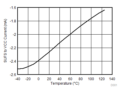
| ISUFS | Charging current into VCC | SUFS = 7.5 V, VCC = 4 V | –1 | –2 | –4 | mA |
| VCCSB(start) | In Self Bias mode, the controller will not start PFC and LLC gate drive outputs until the start up FET has charged the capacitance on the VCC pin above this level | MD_SEL/PS_ON = VCC at power-up (self bias mode) | 15.0 | 16.2 | 17.4 | V |
| VCCSB_UVLO(stop) | In Self Bias mode, VCC must be greater than this level to allow the controller to continue to output the PFC and LLC gate drives. | VCC falling Self Bias Mode | 7.3 | 7.9 | 8.5 | |
| VCC Bias Supply (Aux Bias Mode) | ||||||
| VCCSTART(1) | Controller logic starts at this VCC voltage | VCC rising | 4.4 | 6 | 7.0 | V |
| VCCSTOP(1) | Controller logic stops at this VCC voltage | VCC falling | 3.7 | 5.0 | 5.8 | |
| VCCAB_UVLO(start) | In Aux Bias Mode, VCC must be greater than this level to allow the controller to start the PFC and LLC gate drive outputs. | VCC rising MD_SEL/PS_ON = 0 V at power-up (Aux Bias Mode) | 10.0 | 10.5 | 10.9 | |
| VCCAB_UVLO(stop) | In Aux Bias Mode, VCC must be greater than this level to allow the controller to continue to output the PFC and LLC gate drives. | VCC falling Aux Bias Mode | 9.1 | 9.6 | 10.0 | |
| VCC Supply Current | ||||||
| ICCENABLE | Device is Enabled and providing PFC & LLC gate drive outputs | GD1, GD2 at LLCFMAX. PFC_GD at fPFC (100 kHz nom). GD1, GD2 and PFC_GD pins unloaded. | 7.5 | 8.0 | 18.3 | mA |
| MD_SEL/PS_ON, Mode Select Function at Power Up | ||||||
| VMODE_SELSB | Minimum voltage on the MD_SEL/PS_ON pin that will select Self Bias mode on power up (see Device Functional Modes). | 1.1 | 1.6 | 2.1 | V | |
| TMODE_SEL_READ | After VCC pin exceeds VCCSTART. This is the minimum time that the MD_SEL/PS_ON pin must remain below VMODE_SELSB to ensure that Aux Bias Mode is selected (see Device Functional Modes). | 10 | ms | |||
| MD_SEL/PS_ON, Power Supply On Function, Aux Bias Mode Only | ||||||
| VPS_ONPFC_RUN | Minimum voltage on the MD_SEL/PS_ON pin that causes PFC stage to run(2) | 20 | 25 | 33 | %VCC | |
| VPS_ONLLCPFC_RUN | Minimum voltage on the MD_SEL/PS_ON pin that causes PFC and LLC stages to run(2) | 66 | 75 | 85 | %VCC | |
| AC_DET | ||||||
| VOH_TP_LZ | AC_DET output high | I(AC_DET) = –1 mA | 2.5 | 3.1 | 4.1 | V |
| VOL | AC_DET output low | I(AC_DET) = 1 mA | 19 | 35 | 80 | mV |
| IO(max_source) | AC_DET source current | VOUT > 2.4 V | –1.6 | mA | ||
| IO(max_sink) | AC_DET sink current | VOUT< 0.5 V | 6.0 | mA | ||
| VBULK, PFC OUTPUT VOLTAGE | ||||||
| VBULK(ovp) | PFC output overvoltage protection (auto recovery) | 1.06 | 1.10 | 1.14 | V | |
| VBULK(reg) | VBULK regulation set-point | 0.907 | 0.940 | 0.973 | V | |
| VBULK(llc_start) | LLC operation start threshold | 0.70 | 0.73 | 0.77 | V | |
| VBULK(llc_stop) | LLC operation stop threshold | 0.45 | 0.49 | 0.53 | V | |
| AC1, AC2, AC LINE SENSING FOR PFC | ||||||
| RAC1 | AC1 pin resistance to AGND | AC1 pin | 45 | 60 | 71 | kΩ |
| RAC2 | AC2 pin resistance to AGND | AC2 pin | 45 | 60 | 71 | |
| IAC(det)(3)(7) | AC_DET is active HIGH when IAC is below this level | Force current into AC1 or AC2 pins. Unused pin input at 0 V. | 7.03 | 7.48 | 7.93 | µARMS |
| IAC(low_falling)(3)(7) | PFC stage stops 100 ms after IAC is at or below this level | Force current into AC1 or AC2 pins. Unused pin input at 0 V. | 7.03 | 7.48 | 7.93 | |
| IAC(low_rising)(3)(7) | PFC stage is allowed to start when IAC is at or above this level | Force current into AC1 or AC2 pins. Unused pin input at 0 V. | 8.04 | 8.55 | 9.1 | |
| IAC(high_falling)(3)(7) | PFC stage restarts if IAC falls below this level. No soft-start | Force current into AC1 or AC2 pins. Unused pin input at 0 V. | 30.7 | 32.0 | 33.3 | |
| IAC(high_rising)(3)(7) | PFC stage stops if IAC is at or above this level | Force current into AC1 or AC2 pins. Unused pin input at 0 V. | 31.8 | 33.1 | 34.4 | |
| IAC(halt)(3)(7) | PFC and LLC stages stop if IAC is at or above this level | Force current into AC1 or AC2 pins. Unused pin input at 0 V. | 32.8 | 34.2 | 35.6 | |
| PFC_CS, PFC CURRENT SENSE | ||||||
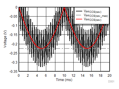
| VPFCCS(cav_max) | Maximum voltage at PFC_CS pin, (ignoring signal ripple due to inductor ripple current) that determines maximum power delivered. Used to determine RCS_PFC. (see PFC Stage Current SensingFigure 13 and Figure 6) | –200 | –225 | –250 | mV | |
| VPFCCS(max) | Maximum voltage at PFC_CS pin | VBULK pin = 800 mV, |VAC1 – VAC2| = VAC_PEAK(4) | –570 | –800 | –950 | |
| PFC_GD, PFC GATE DRIVER | ||||||
| VHI(pfc_2mA) | PFC_GD high level | IO(PFC_GD) = –2 mA | 11.5 | 11.8 | 12.0 | V |
| VHI(pfc_75mA) | PFC_GD high level | IO(PFC_GD) = –75 mA | 8.5 | 9.5 | 10.5 | |
| RPFC(gd_hi) | PFC_GD pull-up resistance | IO(PFC_GD) = –50 mA | 14 | 25 | Ω | |
| RPFC(gd_lo) | PFC_GD pull-down resistance | IO(PFC_GD) = 75 mA | 4.4 | 10 | ||
| tR(pfc) | PFC_GD rise time | Capacitive load of 1.0 nF on PFC_GD pin, 20% to 80% | 30 | 45 | ns | |
| tF(pfc) | PFC_GD fall time | Capacitive load of 1.0 nF on PFC_GD pin, 20% to 80% | 10 | 25 | ||
| fPFC | Switching frequency | Includes dithering of ±2 kHz at nominal 333-Hz rate. | 87 | 98 | 109 | kHz |
| FB, LLC Control Loop Feedback | ||||||
| VFB(min)(8) | Minimum voltage on FB pin where LLC frequency is modulated | Below VFB_MIN, LLC frequency is LLCFmin | 0.17 | 0.2 | 0.23 | V |
| VFB(max)(8) | Maximum voltage on FB pin where LLC frequency is modulated | Between VFB_MAX, and VFB_LLC_OFF LLC frequency is LLCFmax | 2.90 | 3 | 3.10 | |
| VFB(llc_off)(8) | Voltage on FB pin above which LLC gate drive terminated | Once VFB exceeds VFB_LLC_OFF, VFB must fall below VFB_MAX to resume switching | 3.62 | 3.75 | 3.88 | |
| LLCFMIN(8) | Minimum LLC switching frequency | 63.7 | 70 | 74.8 | kHz | |
| LLCFMAX(8) | Maximum LLC switching frequency | 321 | 350 | 378 | ||
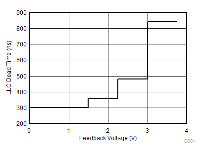
| LLCT(dead)(9) | Time for which GD1 and GD2 are both low during LLC operation at LLCFMIN | LLC dead-time at minimum switching frequency. | 224 | 300 | 388 | ns |
| RFB | Internal resistance from FB pin to AGND | 45 | 60 | 71 | kΩ | |
| LLC_CS, LLC Current Sense | ||||||
| VCS(ocp3)(10) | LLC Overcurrent threshold level three | If this level is exceeded the PFC and LLC stages will stop for tLONG(fault). Restart with a normal soft-start sequence | 0.87 | 0.9 | 0.94 | V |
| VCS(llc_max) | Voltage at LLC_CS pin at 100% of full load | 0.27 | 0.30 | 0.33 | ||
| FAULT Section | ||||||
| tLONG(fault) | Recovery time after long fault | 0.9 | 1.0 | 1.5 | s | |
| tSHORT(fault) | Recovery time after short fault | 90 | 100 | 150 | ms | |
| GD1, GD2, LLC GATE Drive Output | ||||||
| VGD(hi_2mA) | GD1, GD2 output high level | IO(GDx) = –2 mA | 11.5 | 11.8 | 12 | V |
| VGD(hi_75mA) | GD1, GD2 output high level | IO(GDx) = –75 mA | 9.3 | 10.1 | 10.9 | |
| RGD(hi) | GD1, GD2 gate driver pull-up resistance | IO(GDx) = –50 mA | 5.8 | 10.5 | Ω | |
| RGD(lo) | GD1, GD2 gate driver pull-down resistance | IO(GDx) = 75 mA | 1.6 | 5 | ||
| tr(llcgd) | LLC gate driver rise time | Capacitive load of 1 nF on GD1, GD2 pins | 12 | 30 | ns | |
| tf(llcgd) | LLC gate driver fall time | capacitive load of 1 nF on GD1, GD2 pins (20% to 80%) | 11 | 25 | ||
| Thermal Shutdown | ||||||
| TSD | Thermal shutdown temperature | 125 | °C | |||
| TST | Start / restart temperature | 113 | ||||
(1) VCCSTARTis always greater than VCCSTOP.
(2) Threshold voltage will track VCC and is therefore specified as a percentage of VCC.
(3) These are specified at 25°C. The relative levels for these specifications track each other. The equivalent line voltages are given in Table 3, assuming a source impedance of 9.3 MΩ.
(4) Tested at peak of line voltage or 90° from zero crossing.
(5) The device has been characterized over the entire temperature range during development. Individual devices may enter temperature shutdown (TSD) at TJ lower than 125°C.
(6) The device has been characterized over the entire temperature range during development. Individual devices may enter temperature shutdown (TSD) at TJ lower than 125°C.
(8) Refer to Figure 1.
(9) Refer to Figure 2.
(10) Refer to Table 4 for other LLC Stage Over-Current Protection Levels.
6.7 Typical Characteristics
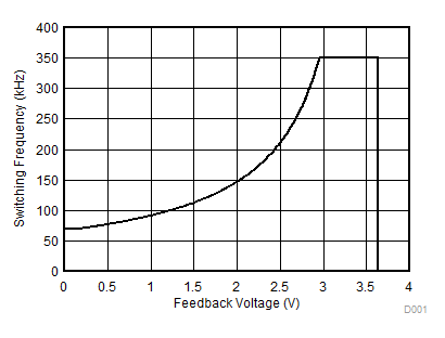
A.
Figure 1. LLC Switching Frequency vs VFB
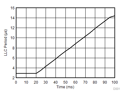
A.
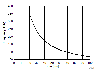
Figure 3. LLC Period vs Time During Soft-Start
