SLVSCS1B March 2015 – May 2015 UCD7138
PRODUCTION DATA.
- 1 Features
- 2 Applications
- 3 Description
- 4 Simplified Schematic
- 5 Revision History
- 6 Pin Configuration and Functions
- 7 Specifications
- 8 Detailed Description
- 9 Application and Implementation
- 10Power Supply Recommendations
- 11Layout
- 12Device and Documentation Support
- 13Mechanical, Packaging, and Orderable Information
Package Options
Mechanical Data (Package|Pins)
- DRS|6
Thermal pad, mechanical data (Package|Pins)
Orderable Information
8 Detailed Description
8.1 Overview
The UCD7138 low-side gate driver is a high-performance driver for secondary-side synchronous rectification with body-diode conduction sensing. The device is suitable for high-power high-efficiency isolated converter applications where dead-time optimization is desired. The body-diode conduction is sensed at the falling edge of the gate-drive signal and sent to the UCD3138A digital-power controller through one digital IO pin. The digital controller can adjust the dead-time setting based on this information. The body-diode conduction time is detected in a certain time window in the UCD3138A digital controller. This detection prevents reporting erroneous signals because of noise or reverse current. At the gate turnon edge, the UCD7138 gate driver optimizes the dead time by turning the gate on as soon as diode conduction is detected. The benefits of this driver to the system include, but are not limited to, improved efficiency, improved reliability, and ease of design.
The internal gate driver is a single-channel, high-speed gate driver suitable for both 12-V and 5-V drive. The gate driver offers 4-A source and 6-A sink (asymmetrical drive) peak drive current capability. The package and pin configuration provide minimum parasitic inductances to reduce rise and fall times and to limit ringing. Additionally, the short propagation delay with minimized tolerances and variations allows efficient operation at high frequencies. The 5-Ω and 0.35-Ω pull-up and pull-down resistances boost immunity to hard switching with high slew-rate dV and dt.
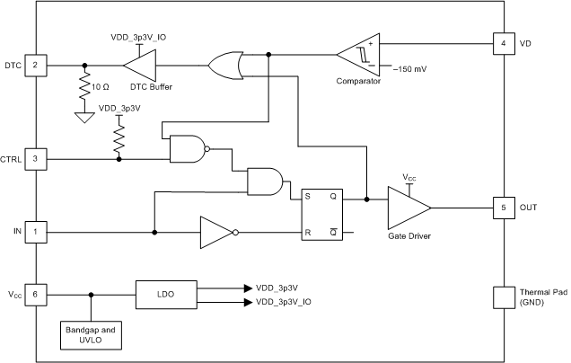
The internal body-diode conduction detector is a high-speed comparator with 20-ns propagation delay. The DTC output is internally pulled high by default. When body-diode conduction is sensed, DTC pin drives low.
8.2 Functional Block Diagram

8.3 Feature Description
8.3.1 Body-Diode Conduction Detection
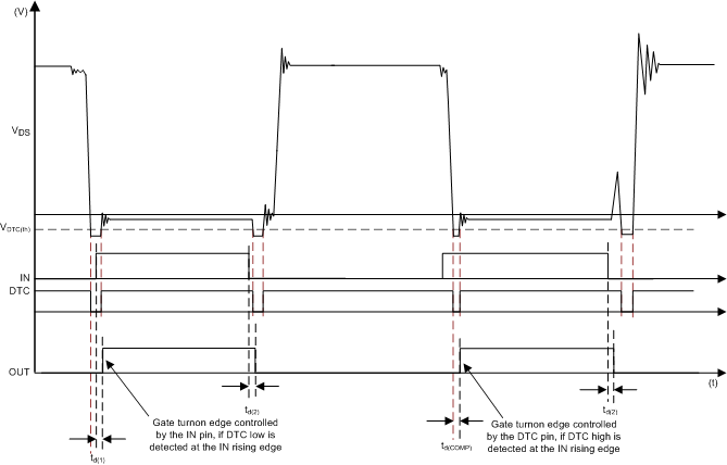
In Figure 24, VDS is the drain-to-source voltage which is connected to the VD pin. The IN pin is the gate-driver input-command signal from the UCD3138A digital controller. The DTC pin is the sensed body-diode conduction. The OUT pin is the gate-driver output. The body-diode conduction detection comparator has a –150-mV threshold. When the body diode conducts, the DTC pin is low. If the body diode does not conduct, the DTC pin is high.
 Figure 24. Input-Output Timing Diagram (Turn-On Optimization is Enabled)
To improve noise immunity, the comparator output DTC is blanked when the gate driver output, OUT, is high. The DTC signal always outputs high when OUT is high.
8.3.2 Gate Turnon and Turnoff
Gate turnon is controlled by both the gate driver input, IN, and body-diode conduction. System robustness is enhanced through internal logic that guarantees that OUT is only allowed high if IN is also high. At the IN rising edge, the UCD7138 gate-driver analyzes the DTC signal and determines the required course of action. The OUT pin is sent high immediately if the DTC comparator output is low at the rising edge of the IN signal. If the DTC pin is high at the rising edge of the IN signal, OUT is held low until DTC goes low. To allow the gate turnon edge to optimize freely, setting the dead time between the primary side falling edge and the IN rising edge smaller than expected in the UCD3138A digital controller is recommended.
The gate turnoff edge is determined by the IN signal only. The gate is turned off immediately at the IN falling edge.
Table 1. Truth Table for CTRL Pin Function
| CTRL PIN CONFIGURATION | FUNCTION |
|---|---|
| 0 V or ground | Turn-on optimization disabled |
| 3.3 V or floating | Turn-on optimization enabled |
8.3.3 VCC and Undervoltage Lockout
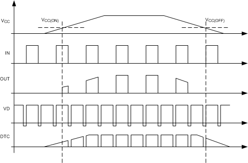
The UCD7138 device has an internal undervoltage-lockout (UVLO) protection feature based on the VCC-pin voltage. Whenever the driver is in the UVLO condition (such as when the VCC voltage is less than VCC(ON) during power up or when the VCC voltage is less than VCC(OFF) during power down), the device holds all outputs low, regardless of the status of the inputs. The UVLO voltage is typically 3.8 V with a 240-mV hysteresis. This hysteresis helps prevent chatter when low VCC supply voltages have noise from the power supply and also when droops occur in the VCC bias voltage.
For example, at power up, the UCD7138 driver output remains low until the VCC voltage reaches the UVLO threshold. The magnitude of the OUT signal rises with VCC until steady-state VCC is reached. The output remains low until the UVLO threshold is reached. The DTC signal begins to rise when VCC begins to rise. The internal diode conduction detection comparator remains inactive until VCC passes VCC(ON) threshold.
 Figure 25. Device Power Up and Power Down
8.3.4 Operating Supply Current
The UCD7138 device features very-low quiescent supply current. The total supply current is the sum of the quiescent supply current, the average IOUT current from switching, and any current related to pull-up resistors on the unused input pin. Knowing the operating frequency (ƒS) and the MOSFET gate (QG) charge, the average IOUT current can be calculated as product of QG and ƒS.
8.3.5 Driver Stage
The input pins of the UCD7138 device are based on a CMOS-compatible input-threshold logic that is independent of the VCC supply voltage. The logic-level thresholds can be conveniently driven with PWM control signals derived from 3.3-V.
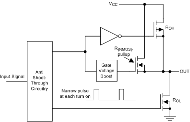
The output stage of the UCD7138 device features a unique architecture on the pull-up structure. This architecture delivers the highest peak-source current when needed during the Miller-plateau region of the power switch turnon transition (when the power switch drain or collector voltage experiences dV/dt). The output stage pull-up structure features a P-Channel MOSFET and an additional N-Channel MOSFET in parallel. The function of the N-Channel MOSFET is to provide a brief boost in the peak sourcing current to enable fast turnon. This boost occurs by briefly turning on the N-Channel MOSFET when the output is changing state from LOW to HIGH.
 Figure 26. Gate-Driver Output Structure
8.4 Device Functional Modes
8.4.1 UVLO Mode
When the VCC voltage to the device has not reached the VCC(ON) threshold or has fallen below the UVLO threshold, VCC(OFF) , the device operates in the low-power UVLO mode. In this mode, most internal functions are disabled and the ICC current is very low. In UVLO mode, the OUT pin is held low. The device passes out of UVLO mode when the VCC voltage increases above the VCC(ON) threshold.
8.4.2 Normal Operation Mode
In this mode, the ICC current is higher because all internal control and timing functions are operating and the gate-driver output, OUT, is driving the controlled MOSFET for synchronous rectification. In this mode, the VCC current is the sum of ICC(ON) plus the average current required to drive the load on the OUT pin.