SLVSDD4C September 2016 – March 2020 UCD90160A
PRODUCTION DATA.
- 1 Features
- 2 Applications
- 3 Description
- 4 Revision History
- 5 Pin Configuration and Functions
- 6 Specifications
-
7 Detailed Description
- 7.1 Overview
- 7.2 Functional Block Diagram
- 7.3 Feature Description
- 7.4
Device Functional Modes
- 7.4.1 Power Supply Sequencing
- 7.4.2 Pin-Selected Rail States
- 7.4.3 Voltage Monitoring
- 7.4.4 Fault Responses and Alert Processing
- 7.4.5 Shut Down All Rails and Sequence On (Resequence)
- 7.4.6 GPIOs
- 7.4.7 GPO Control
- 7.4.8 GPO Dependencies
- 7.4.9 GPI Special Functions
- 7.4.10 Power Supply Enables
- 7.4.11 Cascading Multiple Devices
- 7.4.12 PWM Outputs
- 7.4.13 Programmable Multiphase PWMs
- 7.4.14 Margining
- 7.4.15 System Reset Signal
- 7.4.16 Watch Dog Timer
- 7.4.17 Run Time Clock
- 7.4.18 Data and Error Logging to Flash Memory
- 7.4.19 Brownout Function
- 7.4.20 PMBus Address Selection
- 7.4.21 Device Reset
- 7.5 Programming
- 8 Application and Implementation
- 9 Power Supply Recommendations
- 10Layout
- 11Device and Documentation Support
- 12Mechanical, Packaging, and Orderable Information
Package Options
Mechanical Data (Package|Pins)
- RGC|64
Thermal pad, mechanical data (Package|Pins)
- RGC|64
Orderable Information
3 Description
The UCD90160A is a 16-rail PMBus/I2C addressable power supply sequencer and monitor. The device integrates a 12-bit ADC for monitoring up to 16 power supply voltage inputs. Twenty-six GPIO pins can be used for power supply enables, power-on reset signals, external interrupts, cascading, or other system functions. Twelve of these pins offer PWM functionality. Using these pins, the UCD90160A offers support for margining, and general-purpose PWM functions.
Specific power states can be achieved using the Pin-Selected Rail States feature. This feature allows with the use of up to 3 GPIs to enable and disable any rail. This is useful for implementing system low-power modes and the Advanced Configuration and Power Interface (ACPI) specification that is used for hardware devices.
The Fault Pin feature enables easily cascading multiple devices and coordinates among those devices to take synchronized fault responses.
The TI Fusion Digital Power™ designer software is provided for device configuration. This PC-based graphical user interface (GUI) offers an intuitive interface for configuring, storing, and monitoring all system operating parameters.
Device Information(1)
| PART NUMBER | PACKAGE | BODY SIZE (NOM) |
|---|---|---|
| UCD90160A | VQFN (64) | 9.00 mm × 9.00 mm |
- For all available packages, see the orderable addendum at the end of the data sheet.
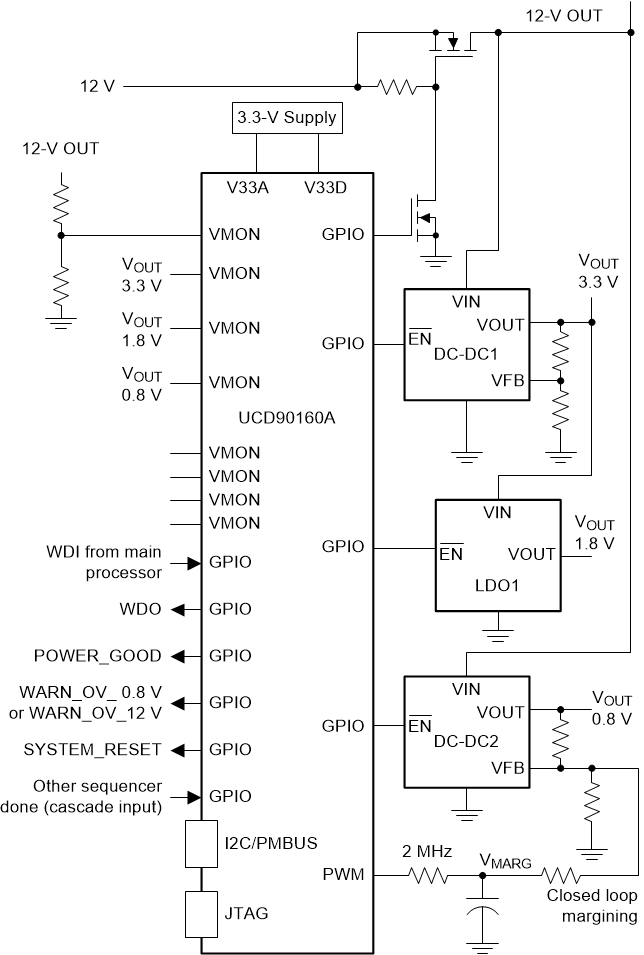
Simplified Application
