SLES275A January 2015 – December 2017 VSP5324-Q1
PRODUCTION DATA.
- 1 Features
- 2 Applications
- 3 Description
- 4 Revision History
- 5 Pin Configuration and Functions
-
6 Specifications
- 6.1 Absolute Maximum Ratings
- 6.2 ESD Ratings
- 6.3 Recommended Operating Conditions
- 6.4 Thermal Information
- 6.5 Electrical Characteristics: Dynamic Performance
- 6.6 Electrical Characteristics: General
- 6.7 Electrical Characteristics: Digital
- 6.8 Timing Requirements
- 6.9 LVDS Timing at Different Sampling Frequencies (One-Lane Interface, 12x Serialization)
- 6.10 LVDS Timing at Different Sampling Frequencies (Two-Lane Interface, 6x Serialization)
- 6.11 Serial Interface Timing Requirements
- 6.12 Typical Characteristics
-
7 Detailed Description
- 7.1 Overview
- 7.2 Functional Block Diagrams
- 7.3 Feature Description
- 7.4 Device Functional Modes
- 7.5 Programming
- 7.6
Register Maps
- 7.6.1
Serial Registers
- 7.6.1.1 Register 00h (offset = 00h) [reset = 0]
- 7.6.1.2 Register 01h (offset = 01h) [reset = 0]
- 7.6.1.3 Register 02h (offset = 02h) [reset = 0]
- 7.6.1.4 Register 0Ah (offset = 0Ah) [reset = 0]
- 7.6.1.5 Register 0Fh (offset = 0Fh) [reset = 0]
- 7.6.1.6 Register 14h (offset = 14h) [reset = 0]
- 7.6.1.7 Register 1Ch (offset = 1Ch) [reset = 0]
- 7.6.1.8 Register 23h (offset = 23h) [reset = 0]
- 7.6.1.9 Register 24h (offset = 24h) [reset = 0]
- 7.6.1.10 Register 25h (offset = 25h) [reset = 0]
- 7.6.1.11 Register 26h (offset = 26h) [reset = 0]
- 7.6.1.12 Register 27h (offset = 27h) [reset = 0]
- 7.6.1.13 Register 28h (offset = 28h) [reset = 0]
- 7.6.1.14 Register 29h (offset = 29h) [reset = 0]
- 7.6.1.15 Register 2Ah (offset = 2Ah) [reset = 0]
- 7.6.1.16 Register 2Bh (offset = 2Bh) [reset = 0]
- 7.6.1.17 Register 2Eh (offset = 2Eh) [reset = 0]
- 7.6.1.18 Register 30h (offset = 30h) [reset = 0]
- 7.6.1.19 Register 33h (offset = 33h) [reset = 0]
- 7.6.1.20 Register 35h (offset = 35h) [reset = 0]
- 7.6.1.21 Register 38h (offset = 38h) [reset = 0x0000]
- 7.6.1.22 Register 42h (offset = 42h) [reset = 0]
- 7.6.1.23 Register 45h (offset = 45h) [reset = 0]
- 7.6.1.24 Register 46h (offset = 46h) [reset = 0]
- 7.6.1.25 Register 50h (offset = 50h) [reset = 0]
- 7.6.1.26 Register 51h (offset = 51h) [reset = 0]
- 7.6.1.27 Register 53h (offset = 53h) [reset = 0]
- 7.6.1.28 Register 54h (offset = ) [reset = 0]
- 7.6.1.29 Register 55h (offset = 55h) [reset = 0]
- 7.6.1.30 Register F0h (offset = F0h) [reset = 0]
- 7.6.1
Serial Registers
- 8 Application and Implementation
- 9 Power Supply Recommendations
- 10Layout
- 11Device and Documentation Support
- 12Mechanical, Packaging, and Orderable Information
Package Options
Mechanical Data (Package|Pins)
- RGC|64
Thermal pad, mechanical data (Package|Pins)
- RGC|64
Orderable Information
1 Features
- Qualified for Automotive Applications
- AEC-Q100 Qualified With the Following Results
- Device Temperature Grade 2: –40°C to +105°C
- Device HBM ESD Classification Level 2
- Device CDM ESD Classification Level C4B
- Designed for Low Power:
- One-Lane Interface:
65 mW per Channel at 50 MSPS - Two-Lane Interface:
82 mW per Channel at 80 MSPS
- One-Lane Interface:
- Dynamic Performance:
- 5-MHz Input Frequency, 80 MSPS
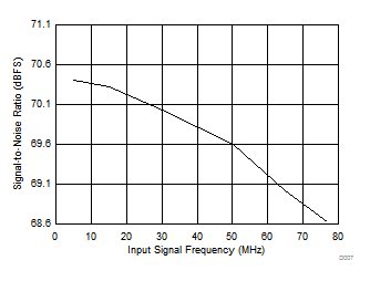
- SNR: 70 dBFS
- SFDR: 85 dBc
- Serial LVDS ADC Data Outputs
- Variety of LVDS Test Patterns to Verify Data Capture
- Package: 9-mm × 9-mm VQFN-64
- Operating Temperature: –40°C to +105°C
2 Applications
- Depth Sensing:
- Location and Proximity Sensing
- 3D Scanning
- 3D Machine Vision
- Security and Surveillance
- Gesture Controls
3 Description
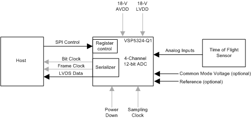
The VSP5324-Q1 device is a low-power, 12-bit, 80-MSPS, quad-channel, analog-to-digital converter (ADC). Low-power consumption and multiple-channel integration in a compact package makes the device attractive for 3D time-of-flight (ToF) systems.
Serial low-voltage differential signaling (LVDS) outputs reduce the number of interface lines and enable high system integration.
The device is available in a compact 9-mm × 9-mm VQFN-64 Package.
Device Information(1)
| PART NUMBER | PACKAGE | BODY SIZE (NOM) |
|---|---|---|
| VSP5324-Q1 | VQFN (64) | 9.00 mm × 9.00 mm |
- For all available packages, see the orderable addendum at the end of the datasheet.
Simplified Schematic

Signal-to-Noise Ratio vs Input Signal Frequency
