SNLS432C October 2012 – December 2015 DS125MB203
PRODUCTION DATA.
- 1 Features
- 2 Applications
- 3 Description
- 4 Revision History
- 5 Description continued
- 6 Pin Configuration and Functions
- 7 Specifications
- 8 Detailed Description
- 9 Application and Implementation
- 10Power Supply Recommendations
- 11Layout
- 12Device and Documentation Support
- 13Mechanical, Packaging, and Orderable Information
Package Options
Mechanical Data (Package|Pins)
- NJY|54
Thermal pad, mechanical data (Package|Pins)
Orderable Information
1 Features
- 12.5-Gbps Dual Lane 2:1 Mux, 1:2 Switch or Fanout
- Low 390-mW Total Power (Typical)
- Advanced Signal Conditioning Features:
- Receive Equalization up to 30 dB at 6.25 GHz
- Transmit De-Emphasis up to –12 dB
- Transmit Output-Voltage Control: 600 mV to 1300 mV
- Programmable Through Pin Selection, EEPROM or SMBus Interface
- Selectable 2.5-V or 3.3-V Supply Voltage
- –40°C to +85°C Operating Temperature Range
2 Applications
- 10GE, 10G-KR
- PCIe Gen-1/2/3
- SAS2/SATA3 (Up to 6 Gbps)
- XAUI, RXAUI
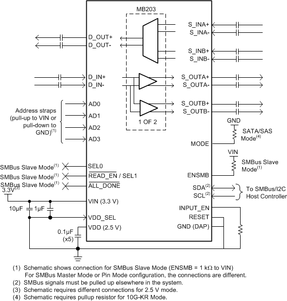
Simplified Functional Block Diagram

3 Description
The DS125MB203 device is a dual port 2:1 multiplexer and 1:2 switch or fan-out buffer with signal conditioning suitable for 10GE, 10G-KR (802.3ap), Fibre Channel, PCIe, Infiniband, SATA3/SAS2 and other high-speed bus applications with data rates up to 12.5 Gbps. The continuous time linear equalizer (CTLE) of the receiver provides necessary boost to compensate up to 30-inch FR-4 or 8-m cable (AWG-24) at 12.5 Gbps. This on-chip feature eliminates the need for external signal conditioners. The transmitter features a programmable amplitude voltage levels to be selectable from 600 mVp-p to 1300 mVp-p and de-emphasis of up to 12 dB.
The DS125MB203 can be configured to support PCIe, SAS/SATA, 10G-KR or other signaling protocols. When operating in 10G-KR and PCIe Gen-3 mode, the DS125MB203 transparently allows the host controller and the end point to optimize the full link and negotiate transmit equalizer coefficients. This seamless management of the link training protocol ensures system level interoperability with minimum latency.
Device Information(1)
| PART NUMBER | PACKAGE | BODY SIZE (NOM) |
|---|---|---|
| DS125MB203 | WQFN (54) | 10.00 mm × 5.50 mm |
- For all available packages, see the orderable addendum at the end of the data sheet.
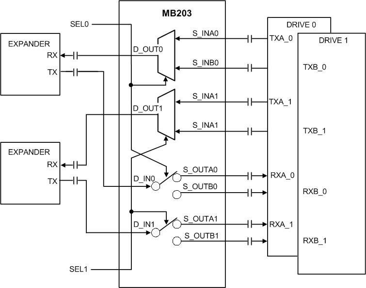
Typical Application
