SNLS498A November 2015 – December 2015 DS90CR286AT-Q1
PRODUCTION DATA.
- 1 Features
- 2 Applications
- 3 Description
- 4 Revision History
- 5 Pin Configuration and Functions
- 6 Specifications
- 7 Detailed Description
- 8 Application and Implementation
- 9 Power Supply Recommendations
- 10Layout
- 11Device and Documentation Support
- 12Mechanical, Packaging, and Orderable Information
Package Options
Mechanical Data (Package|Pins)
- DGG|56
Thermal pad, mechanical data (Package|Pins)
Orderable Information
1 Features
- 20 to 66 MHz Shift Clock Support
- 50% Duty Cycle on Receiver Output Clock
- Best–in–Class Setup & Hold Times on Rx Outputs
- Rx Power Consumption < 270 mW (typ) at 66 MHz Worst Case
- Rx Power-down Mode < 200 μW (max)
- ESD Rating: 4 kV (HBM), 1 kV (CDM)
- PLL Requires No External Components
- Compatible with TIA/EIA-644 LVDS Standard
- Low Profile 56-Pin DGG (TSSOP) Package
- Operating Temperature: −40°C to +105°C
- Automotive AEC-Q100 Grade 2 Qualified
2 Applications
- Video Displays
- Automotive Infotainment
- Industrial Printers and Imaging
- Digital Video Transport
- Machine Vision
- OpenLDI-to-RGB Bridge
3 Description
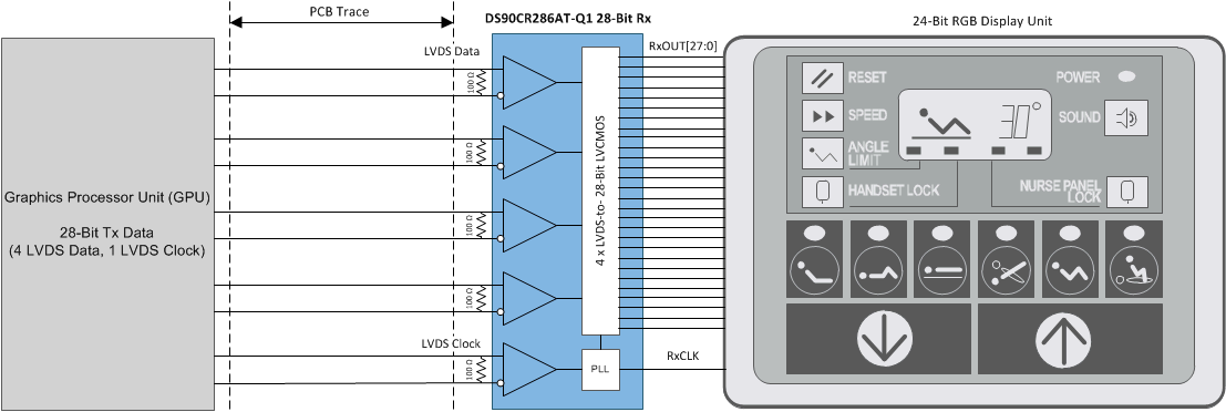
The DS90CR286AT-Q1 receiver converts four LVDS (Low Voltage Differential Signaling) data streams back into parallel 28 bits of LVCMOS data. The receiver data outputs strobe on the output clock's rising edge.
The receiver LVDS clock operates at rates from 20 to 66 MHz. The DS90CR286AT-Q1 phase-locks to the input LVDS clock, samples the serial bit streams at the LVDS data lines, and converts them into 28-bit parallel output data. At an incoming clock rate of 66 MHz, each LVDS input line is running at a bit rate of 462 Mbps, resulting in a maximum throughput of 1.848 Gbps.
The DS90CR286AT-Q1 device is enhanced over prior generation receivers due to a wider data valid time on the receiver output. The DS90CR286AT-Q1 is designed for PCB board chip-to-chip OpenLDI-to-RGB bridge conversion. LVDS data transmission over cable interconnect is not recommended for this device.
Users designing a sub-system with a compatible OpenLDI transmitter and DS90CR286AT-Q1 receiver must ensure an acceptable skew margin budget (RSKM). Details regarding RSKM can be found in the Application Information section.
Device Information(1)
| PART NUMBER | PACKAGE | BODY SIZE (NOM) |
|---|---|---|
| DS90CR286AT-Q1 | TSSOP (56) | 14.00 mm × 6.10 mm |
- For all available packages, see the orderable addendum at the end of the data sheet.
Typical Application Block Diagram
