SBOS770A May 2017 – June 2017 INA826S
PRODUCTION DATA.
- 1 Features
- 2 Applications
- 3 Description
- 4 Revision History
- 5 Pin Configuration and Functions
- 6 Specifications
- 7 Detailed Description
- 8 Application and Implementation
- 9 Power Supply Recommendations
- 10Layout
- 11Device and Documentation Support
- 12Mechanical, Packaging, and Orderable Information
Package Options
Mechanical Data (Package|Pins)
- DRC|10
Thermal pad, mechanical data (Package|Pins)
- DRC|10
Orderable Information
1 Features
- Input Common-Mode Range: Includes V–
- Common-Mode Rejection:
- 104 dB (Min, G = 10)
- 100 dB (Min at 5 kHz, G = 10)
- Power-Supply Rejection: 100 dB (Min, G = 1)
- Low Offset Voltage: 150 µV, max
- Gain Drift: 1 ppm/°C (G = 1), 35 ppm/°C (G > 1)
- Noise: 18 nV/√Hz, G ≥ 100
- Bandwidth: 1 MHz (G = 1), 60 kHz (G = 100)
- Inputs Protected up to ±40 V
- Rail-to-Rail Output
- Supply Current: 200 µA
- Shutdown Current: 2 µA
- Supply Range:
- Single Supply: 3 V to 36 V
- Dual Supply: ±1.5 V to ±18 V
- Specified Temperature Range:
–40°C to +125°C - Packages: 3-mm × 3-mm VSON
2 Applications
- Industrial Process Controls
- Circuit Breakers
- Battery Testers
- ECG Amplifiers
- Power Automation
- Medical Instrumentation
- Portable Instrumentation
3 Description
The INA826S device is a low-cost instrumentation amplifier that offers extremely low power consumption along with shutdown and operates over a very wide single- or dual-supply range. A single external resistor sets any gain from 1 to 1000. The device offers excellent stability over temperature, even at G > 1, as a result of the low gain drift of only 35 ppm/°C (max).
The INA826S is optimized to provide excellent common-mode rejection ratio of over 100 dB (G = 10) over frequencies up to 5 kHz. At G = 1, the common-mode rejection ratio exceeds 84 dB across the full input common-mode range from the negative supply all the way up to 1 V of the positive supply. Using a rail-to-rail output, the INA826S is well-suited for low voltage operation from a 3-V single supply as well as dual supplies up to ±18 V.
Shutdown pins are provided to reduce supply current below 2 µA. Additional circuitry protects the inputs against overvoltage of up to ±40 V beyond the power supplies by limiting the input currents to less than 8 mA.
The INA826S is available in a 10-pin, 3-mm ×
3-mm VSON surface-mount package. The INA826S is specified over the –40°C to +125°C temperature range.
Device Information(1)
| PART NUMBER | PACKAGE | BODY SIZE (NOM) |
|---|---|---|
| INA826S | VSON (10) | 3.00 mm × 3.00 mm |
- For all available packages, see the orderable addendum at the end of the data sheet.
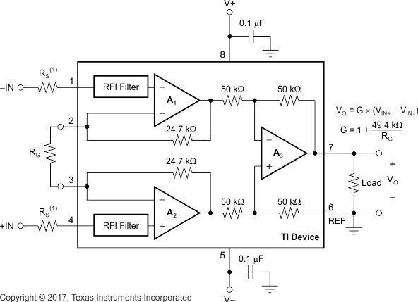
INA826S Simplified Internal Schematic

4 Revision History
Changes from * Revision (May 2017) to A Revision
- Changed output stage offset voltage from 700 µV to 1000 µVGo