JAJSHN0F July 2014 – November 2020 DLPC3430 , DLPC3435
PRODUCTION DATA
- 1 特長
- 2 アプリケーション
- 3 概要
- 4 Revision History
- 5 Pin Configuration and Functions
-
6 Specifications
- 6.1 Absolute Maximum Ratings
- 6.2 ESD Ratings
- 6.3 Recommended Operating Conditions
- 6.4 Thermal Information
- 6.5 Power Electrical Characteristics
- 6.6 Pin Electrical Characteristics
- 6.7 Internal Pullup and Pulldown Electrical Characteristics
- 6.8 DMD Sub-LVDS Interface Electrical Characteristics
- 6.9 DMD Low-Speed Interface Electrical Characteristics
- 6.10 System Oscillator Timing Requirements
- 6.11 Power Supply and Reset Timing Requirements
- 6.12 Parallel Interface Frame Timing Requirements
- 6.13 Parallel Interface General Timing Requirements
- 6.14 BT656 Interface General Timing Requirements
- 6.15 DSI Host Timing Requirements
- 6.16 Flash Interface Timing Requirements
- 6.17 Other Timing Requirements
- 6.18 DMD Sub-LVDS Interface Switching Characteristics
- 6.19 DMD Parking Switching Characteristics
- 6.20 Chipset Component Usage Specification
-
7 Detailed Description
- 7.1 Overview
- 7.2 Functional Block Diagram
- 7.3 Feature Description
- 7.4 Device Functional Modes
- 7.5 Programming
- 8 Application and Implementation
- 9 Power Supply Recommendations
- 10Layout
- 11Device and Documentation Support
- 12Mechanical, Packaging, and Orderable Information
7.3.2 Device Startup
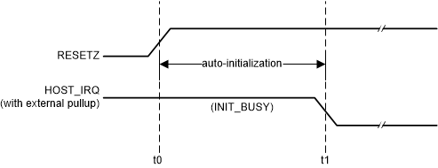
- The HOST_IRQ signal is provided to indicated when the system has completed auto-initialization.
- While reset is applied, HOST_IRQ is tri-stated (an external pullup resistor pulls the line high).
- HOST_IRQ remains tri-stated (pulled high externally) until the boot process completes. While the signal is pulled high, this indicates that the controller is performing boot-up and auto-initialization.
- As soon as possible after the controller boots-up, the controller drives HOST_IRQ to a logic high state to indicate that the controller is continuing to perform auto-initialization (no real state changes occur on the external signal).
- The software sets HOST_IRQ to a logic low state at the completion of the auto-initialization process. At the falling edge of the signal, the initialization is complete.
- The DLPC34xx controller is ready to receive commands through I2C or accept video over the DSI or the parallel interface only after auto-initialization is complete.
- The controller initialization typically completes (HOST_IRQ goes low) within 500 ms of RESETZ being asserted. However, this time may vary depending on the software version and the contents of the user configurable auto initialization file.

t0: rising edge of RESETZ; auto-initialization begins
t1: falling edge of HOST_IRQ; auto-initialization is complete
Figure 7-9 HOST_IRQ Timing