SNAS578D February 2012 – March 2016 LMK00306
PRODUCTION DATA.
- 1 Features
- 2 Applications
- 3 Description
- 4 Revision History
- 5 Pin Configuration and Functions
- 6 Specifications
- 7 Parameter Measurement Information
- 8 Detailed Description
- 9 Application and Implementation
- 10Power Supply Recommendations
- 11Device and Documentation Support
- 12Mechanical, Packaging, and Orderable Information
パッケージ・オプション
デバイスごとのパッケージ図は、PDF版データシートをご参照ください。
メカニカル・データ(パッケージ|ピン)
- NJK|36
サーマルパッド・メカニカル・データ
発注情報
9 Application and Implementation
NOTE
Information in the following applications sections is not part of the TI component specification, and TI does not warrant its accuracy or completeness. TI’s customers are responsible for determining suitability of components for their purposes. Customers should validate and test their design implementation to confirm system functionality.
9.1 Driving the Clock Inputs
The LMK00306 has two universal inputs (CLKin0/CLKin0* and CLKin1/CLKin1*) that can accept AC- or DC-coupled 3.3V/2.5V LVPECL, LVDS, CML, SSTL, and other differential and single-ended signals that meet the input requirements specified in Electrical Characteristics. The device can accept a wide range of signals due to its wide input common mode voltage range (VCM ) and input voltage swing (VID) / dynamic range. For 50% duty cycle and DC-balanced signals, AC coupling may also be employed to shift the input signal to within the VCM range. Refer to Termination and Use of Clock Drivers for signal interfacing and termination techniques.
To achieve the best possible phase noise and jitter performance, it is mandatory for the input to have high slew rate of 3 V/ns (differential) or higher. Driving the input with a lower slew rate will degrade the noise floor and jitter. For this reason, a differential signal input is recommended over single-ended because it typically provides higher slew rate and common-mode-rejection. Refer to the “Noise Floor vs. CLKin Slew Rate” and “RMS Jitter vs. CLKin Slew Rate” plots in Typical Characteristics.
While it is recommended to drive the CLKin/CLKin* pair with a differential signal input, it is possible to drive it with a single-ended clock provided it conforms to the Single-Ended Input specifications for CLKin pins listed in the Electrical Characteristics. For large single-ended input signals, such as 3.3V or 2.5V LVCMOS, a 50 Ω load resistor should be placed near the input for signal attenuation to prevent input overdrive as well as for line termination to minimize reflections. Again, the single-ended input slew rate should be as high as possible to minimize performance degradation. The CLKin input has an internal bias voltage of about 1.4 V, so the input can be AC coupled as shown in Figure 25. The output impedance of the LVCMOS driver plus Rs should be close to 50 Ω to match the characteristic impedance of the transmission line and load termination.
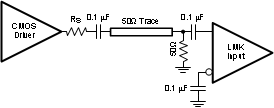 Figure 25. Single-Ended LVCMOS Input, AC Coupling
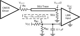
A single-ended clock may also be DC coupled to CLKinX as shown in Figure 26. A 50-Ω load resistor should be placed near the CLKinX input for signal attenuation and line termination. Because half of the single-ended swing of the driver (VO,PP / 2) drives CLKinX, CLKinX* should be externally biased to the midpoint voltage of the attenuated input swing ((VO,PP / 2) × 0.5). The external bias voltage should be within the specified input common voltage (VCM) range. This can be achieved using external biasing resistors in the kΩ range (RB1 and RB2) or another low-noise voltage reference. This will ensure the input swing crosses the threshold voltage at a point where the input slew rate is the highest.
If the LVCMOS driver cannot achieve sufficient swing with a DC-terminated 50Ω load at the CLKinX input as shown in Figure 26, then consider connecting the 50Ω load termination to ground through a capacitor (CAC). This AC termination blocks the DC load current on the driver, so the voltage swing at the input is determined by the voltage divider formed by the source (Ro+Rs) and 50Ω load resistors. The value for CAC depends on the trace delay, Td, of the 50Ω transmission line, where CAC >= 3*Td/50Ω.
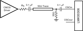
If the crystal oscillator circuit is not used, it is possible to drive the OSCin input with an single-ended external clock as shown in Figure 27. The input clock should be AC coupled to the OSCin pin, which has an internally-generated input bias voltage, and the OSCout pin should be left floating. While OSCin provides an alternative input to multiplex an external clock, it is recommended to use either universal input (CLKinX) since it offers higher operating frequency, better common mode and power supply noise rejection, and greater performance over supply voltage and temperature variations.
9.2 Crystal Interface
The LMK00306 has an integrated crystal oscillator circuit that supports a fundamental mode, AT-cut crystal. The crystal interface is shown in Figure 28.
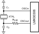 Figure 28. Crystal Interface
The load capacitance (CL) is specific to the crystal, but usually on the order of 18 - 20 pF. While CL is specified for the crystal, the OSCin input capacitance (CIN = 4 pF typical) of the device and PCB stray capacitance (CSTRAY ~ 1~3 pF) can affect the discrete load capacitor values, C1 and C2.
For the parallel resonant circuit, the discrete capacitor values can be calculated as follows:
Typically, C1 = C2 for optimum symmetry, so Equation 1 can be rewritten in terms of C1 only:
Finally, solve for C1:
Electrical Characteristics provides crystal interface specifications with conditions that ensure start-up of the crystal, but it does not specify crystal power dissipation. The designer will need to ensure the crystal power dissipation does not exceed the maximum drive level specified by the crystal manufacturer. Overdriving the crystal can cause premature aging, frequency shift, and eventual failure. Drive level should be held at a sufficient level necessary to start-up and maintain steady-state operation.
The power dissipated in the crystal, PXTAL, can be computed by:
where
- IRMS is the RMS current through the crystal.
- RESR is the max. equivalent series resistance specified for the crystal
- CL is the load capacitance specified for the crystal
- C0 is the min. shunt capacitance specified for the crystal
IRMS can be measured using a current probe (e.g. Tektronix CT-6 or equivalent) placed on the leg of the crystal connected to OSCout with the oscillation circuit active.
As shown in Figure 28 , an external resistor, RLIM, can be used to limit the crystal drive level, if necessary. If the power dissipated in the selected crystal is higher than the drive level specified for the crystal with RLIM shorted, then a larger resistor value is mandatory to avoid overdriving the crystal. However, if the power dissipated in the crystal is less than the drive level with RLIM shorted, then a zero value for RLIM can be used. As a starting point, a suggested value for RLIM is 1.5 kΩ.
9.3 Termination and Use of Clock Drivers
When terminating clock drivers keep in mind these guidelines for optimum phase noise and jitter performance:
- Transmission line theory should be followed for good impedance matching to prevent reflections.
- Clock drivers should be presented with the proper loads.
- LVDS outputs are current drivers and require a closed current loop.
- HCSL drivers are switched current outputs and require a DC path to ground via 50 Ω termination.
- LVPECL outputs are open emitter and require a DC path to ground.
- Receivers should be presented with a signal biased to their specified DC bias level (common mode voltage) for proper operation. Some receivers have self-biasing inputs that automatically bias to the proper voltage level; in this case, the signal should normally be AC coupled.
It is possible to drive a non-LVPECL or non-LVDS receiver with a LVDS or LVPECL driver as long as the above guidelines are followed. Check the datasheet of the receiver or input being driven to determine the best termination and coupling method to be sure the receiver is biased at the optimum DC voltage (common mode voltage).
9.3.1 Termination for DC Coupled Differential Operation
For DC coupled operation of an LVDS driver, terminate with 100 Ω as close as possible to the LVDS receiver as shown in Figure 29.
 Figure 29. Differential LVDS Operation, DC Coupling,
 No Biasing by the Receiver
For DC coupled operation of an HCSL driver, terminate with 50 Ω to ground near the driver output as shown in Figure 30. Series resistors, Rs, may be used to limit overshoot due to the fast transient current. Because HCSL drivers require a DC path to ground, AC coupling is not allowed between the output drivers and the 50 Ω termination resistors.
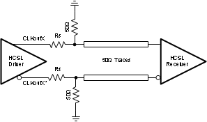 Figure 30. HCSL Operation, DC Coupling
For DC coupled operation of an LVPECL driver, terminate with 50 Ω to Vcco – 2 V as shown in Figure 31. Alternatively terminate with a Thevenin equivalent circuit as shown in Figure 32 for Vcco (output driver supply voltage) = 3.3 V and 2.5 V. In the Thevenin equivalent circuit, the resistor dividers set the output termination voltage (VTT) to Vcco - 2 V.
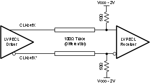 Figure 31. Differential LVPECL Operation, DC Coupling
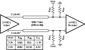 Figure 32. Differential LVPECL Operation, DC Coupling, Thevenin Equivalent
9.3.2 Termination for AC Coupled Differential Operation
AC coupling allows for shifting the DC bias level (common mode voltage) when driving different receiver standards. Since AC coupling prevents the driver from providing a DC bias voltage at the receiver, it is important to ensure the receiver is biased to its ideal DC level.
When driving differential receivers with an LVDS driver, the signal may be AC coupled by adding DC blocking capacitors; however the proper DC bias point needs to be established at both the driver side and the receiver side. The recommended termination scheme depends on whether the differential receiver has integrated termination resistors or not.
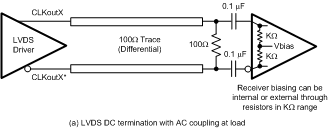
When driving a differential receiver without internal 100 Ω differential termination, the AC coupling capacitors should be placed between the load termination resistor and the receiver to allow a DC path for proper biasing of the LVDS driver. This is shown in Figure 33. The load termination resistor and AC coupling capacitors should be placed as close as possible to the receiver inputs to minimize stub length. The receiver can be biased internally or externally to a reference voltage within the receiver’s common mode input range through resistors in the kilo-ohm range.
When driving a differential receiver with internal 100 Ω differential termination, a source termination resistor should be placed before the AC coupling capacitors for proper DC biasing of the driver as shown in Figure 34. However, with a 100-Ω resistor at the source and the load (i.e. double terminated), the equivalent resistance seen by the LVDS driver is 50 Ω which causes the effective signal swing at the input to be reduced by half. If a self-terminated receiver requires input swing greater than 250 mVpp (differential) as well as AC coupling to its inputs, then the LVDS driver with the double-terminated arrangement in Figure 34 may not meet the minimum input swing requirement; alternatively, the LVPECL or HCSL output driver format with AC coupling is recommended to meet the minimum input swing required by the self-terminated receiver.
When using AC coupling with LVDS outputs, there may be a startup delay observed in the clock output due to capacitor charging. The examples in Figure 33 and Figure 34 use 0.1 μF capacitors, but this value may be adjusted to meet the startup requirements for the particular application.
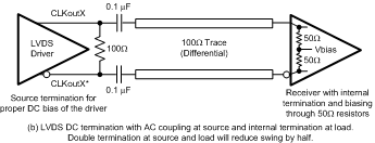 Figure 34. Differential LVDS Operation with AC Coupling to Receivers
With Internal 100 Ω Termination
LVPECL drivers require a DC path to ground. When AC coupling an LVPECL signal use 160 Ω emitter resistors (or 91 Ω for Vcco = 2.5 V) close to the LVPECL driver to provide a DC path to ground as shown in Figure 38. For proper receiver operation, the signal should be biased to the DC bias level (common mode voltage) specified by the receiver. The typical DC bias voltage (common mode voltage) for LVPECL receivers is 2 V. Alternatively, a Thevenin equivalent circuit forms a valid termination as shown in Figure 35 for Vcco = 3.3 V and 2.5 V. Note: this Thevenin circuit is different from the DC coupled example in Figure 32, since the voltage divider is setting the input common mode voltage of the receiver.
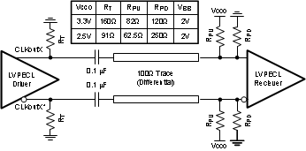 Figure 35. Differential LVPECL Operation, AC Coupling,
 Thevenin Equivalent
9.3.3 Termination for Single-Ended Operation
A balun can be used with either LVDS or LVPECL drivers to convert the balanced, differential signal into an unbalanced, single-ended signal.
It is possible to use an LVPECL driver as one or two separate 800 mV p-p signals. When DC coupling one of the LMK00306 LVPECL driver of a CLKoutX/CLKoutX* pair, be sure to properly terminate the unused driver. When DC coupling on of the LMK00306 LVPECL drivers, the termination should be 50 Ω to Vcco - 2 V as shown in Figure 36. The Thevenin equivalent circuit is also a valid termination as shown in Figure 37 for Vcco = 3.3 V.
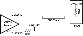 Figure 36. Single-Ended LVPECL Operation, DC Coupling
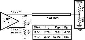 Figure 37. Single-Ended LVPECL Operation, DC Coupling, Thevenin Equivalent
When AC coupling an LVPECL driver use a 160 Ω emitter resistor (or 91 Ω for Vcco = 2.5 V) to provide a DC path to ground and ensure a 50 Ω termination with the proper DC bias level for the receiver. The typical DC bias voltage for LVPECL receivers is 2 V. If the companion driver is not used, it should be terminated with either a proper AC or DC termination. This latter example of AC coupling a single-ended LVPECL signal can be used to measure single-ended LVPECL performance using a spectrum analyzer or phase noise analyzer. When using most RF test equipment no DC bias point (0 VDC) is required for safe and proper operation. The internal 50 Ω termination the test equipment correctly terminates the LVPECL driver being measured as shown in Figure 38. When using only one LVPECL driver of a CLKoutX/CLKoutX* pair, be sure to properly terminated the unused driver.
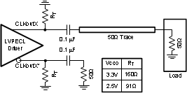 Figure 38. Single-Ended LVPECL Operation, AC Coupling
