SNVS709G March 2011 – December 2015 LMZ13610
PRODUCTION DATA.
- 1 Features
- 2 Applications
- 3 Description
- 4 Revision History
- 5 Pin Configuration and Functions
- 6 Specifications
- 7 Detailed Description
-
8 Application and Implementation
- 8.1 Application Information
- 8.2
Typical Application
- 8.2.1 Design Requirements
- 8.2.2
Detailed Design Procedure
- 8.2.2.1 Design Steps
- 8.2.2.2 Enable Divider, RENT, RENB and RENH Selection
- 8.2.2.3 Output Voltage Selection
- 8.2.2.4 Soft-Start Capacitor Selection
- 8.2.2.5 Tracking Supply Divider Option
- 8.2.2.6 COUT Selection
- 8.2.2.7 CIN Selection
- 8.2.2.8 Discontinuous Conduction and Continuous Conduction Modes Selection
- 8.2.3 Application Curves
- 9 Power Supply Recommendations
- 10Layout
- 11Device and Documentation Support
- 12Mechanical, Packaging, and Orderable Information
8 Application and Implementation
NOTE
Information in the following applications sections is not part of the TI component specification, and TI does not warrant its accuracy or completeness. TI’s customers are responsible for determining suitability of components for their purposes. Customers should validate and test their design implementation to confirm system functionality.
8.1 Application Information
The LMZ13610 is a step-down DC-to-DC power module. It is typically used to convert a higher DC voltage to a lower DC voltage with a maximum output current of 10 A. The following design procedure can be used to select components for the LMZ13610. Alternately, the WEBENCH software may be used to generate complete designs.
When generating a design, the WEBENCH software uses iterative design procedure and accesses comprehensive databases of components. Please go to www.ti.com for more details.
8.2 Typical Application
 Figure 47. Typical Application Schematic
8.2.1 Design Requirements
For this example the following application parameters exist:
- VIN Range = Up to 36 V
- VOUT = 0.8 V to 6 V
- IOUT = 10 A
8.2.2 Detailed Design Procedure
8.2.2.1 Design Steps
The LMZ13610 is fully supported by WEBENCH which offers: component selection, electrical and thermal simulations. Additionally, there are both evaluation and demonstration boards that may be used as a starting point for design. The following list of steps can be used to manually design the LMZ13610 application.
All references to values refer to the Figure 47.
- Select minimum operating VIN with enable divider resistors
- Program VOUT with FB resistor divider selection
- Select COUT
- Select CIN
- Determine module power dissipation
- Layout PCB for required thermal performance
8.2.2.2 Enable Divider, RENT, RENB and RENH Selection
Internal to the module is a 2-MΩ pullup resistor connected from VIN to Enable. For applications not requiring precision undervoltage lockout (UVLO), the Enable input may be left open circuit and the internal resistor will always enable the module. In such case, the internal UVLO occurs typically at 4.3 V (VIN rising).
In applications with separate supervisory circuits Enable can be directly interfaced to a logic source. In the case of sequencing supplies, the divider is connected to a rail that becomes active earlier in the power-up cycle than the LMZ13610 output rail.
Enable provides a precise 1.274-V threshold to allow direct logic drive or connection to a voltage divider from a higher enable voltage such as VIN. Additionally there is 13 μA (typical) of switched offset current allowing programmable hysteresis. See Figure 48.
The function of the enable divider is to allow the designer to choose an input voltage below which the circuit will be disabled. This implements the feature of a programmable UVLO. The two resistors must be chosen based on the following ratio:
The LMZ13610 typical application shows 12.7 kΩ for RENB and 42.2 kΩ for RENT resulting in a rising UVLO of 5.51 V. Note that this divider presents 4.62 V to the EN input when VIN is raised to 20 V. This upper voltage must always be checked, making sure that it never exceeds the Abs Max 5.5-V limit for Enable. A 5.1-V Zener clamp can be applied in cases where the upper voltage would exceed the EN input's range of operation. The Zener clamp is not required if the target application prohibits the maximum Enable input voltage from being exceeded.
Additional enable voltage hysteresis can be added with the inclusion of RENH. It is possible to select values for RENT and RENB such that RENH is a value of zero allowing it to be omitted from the design.
Rising threshold can be calculated as follows:
Whereas the falling threshold level can be calculated using:
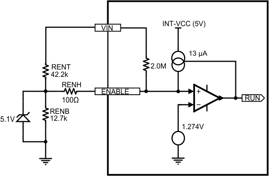 Figure 48. Enable Input Detail
8.2.2.3 Output Voltage Selection
Output voltage is determined by a divider of two resistors connected between VOUT and AGND. The midpoint of the divider is connected to the FB input.
The regulated output voltage determined by the external divider resistors RFBT and RFBB is:
Rearranging terms; the ratio of the feedback resistors for a desired output voltage is:
These resistors must generally be chosen from values in the range of 1.0 kΩ to 10.0 kΩ.
For VOUT = 0.8 V the FB pin can be connected to the output directly and RFBB can be set to 8.06kΩ to provide minimum output load.
Table 1 lists the values for RFBT, and RFBB.
Table 1. Typical Application Bill of Materials
| REF DES | DESCRIPTION | CASE SIZE | MANUFACTURER | MANUFACTURER P/N |
|---|---|---|---|---|
| U1 | SIMPLE SWITCHER | PFM-11 | Texas Instruments | LMZ13610TZ |
| CIN1,6 (OPT) | 0.047 µF, 50 V, X7R | 1206 | Yageo America | CC1206KRX7R9BB473 |
| CIN2,3,4 | 10 µF, 50 V, X7R | 1210 | Taiyo Yuden | UMK325BJ106MM-T |
| CIN5 (OPT) | CAP, AL, 150 µF, 50 V | Radial G | Panasonic | EEE-FK1H151P |
| CO1,5 (OPT) | 0.047 µF, 50 V, X7R | 1206 | Yageo America | CC1206KRX7R9BB473 |
| CO2 (OPT) | 47 µF, 10 V, X7R | 1210 | Murata | GRM32ER61A476KE20L |
| CO3,4 | 330 μF, 6.3V, 0.015 Ω | CAPSMT_6_UE | Kemet | T520D337M006ATE015 |
| RFBT | 3.32 kΩ | 0805 | Panasonic | ERJ-6ENF3321V |
| RFBB | 1.07 kΩ | 0805 | Panasonic | ERJ-6ENF1071V |
| RENT | 42.2 kΩ | 0805 | Panasonic | ERJ-6ENF4222V |
| RENB | 12.7 kΩ | 0805 | Panasonic | ERJ-6ENF1272V |
| CSS | 0.47 μF, ±10%, X7R, 16 V | 0805 | AVX | 0805YC474KAT2A |
| D1 (OPT) | 5.1 V, 0.5 W | SOD-123 | Diodes Inc. | MMSZ5231BS-7-F |
8.2.2.4 Soft-Start Capacitor Selection
Programmable soft-start permits the regulator to slowly ramp to its steady-state operating point after being enabled, thereby reducing current inrush from the input supply and slowing the output voltage rise-time.
Upon turnon, after all UVLO conditions have been passed, an internal 1.6-ms circuit slowly ramps the SS input to implement internal soft-start. If 1.6 ms is an adequate turnon time then the Css capacitor can be left unpopulated. Longer soft-start periods are achieved by adding an external capacitor to this input.
Soft-start duration is given by the formula:
This equation can be rearranged as follows:
Using a 0.22-μF capacitor results in 3.5 ms typical soft-start duration; and 0.47 μF results in 7.5 ms typical. 0.47 μF is a recommended initial value.
As the soft-start input exceeds 0.795 V the output of the power stage will be in regulation and the 50-μA current is deactivated. The following conditions will reset the soft-start capacitor by discharging the SS input to ground with an internal current sink.
- The Enable input being pulled low
- A thermal shutdown condition
- VIN falling below 4.3 V (typical) and triggering the VCC UVLO
8.2.2.5 Tracking Supply Divider Option
The tracking function allows the module to be connected as a slave supply to a primary voltage rail (often the 3.3-V system rail) where the slave module output voltage is lower than that of the master. Proper configuration allows the slave rail to power up coincident with the master rail such that the voltage difference between the rails during ramp-up is small (that is, < 0.15 V typical). The values for the tracking resistive divider must be selected such that the effect of the internal 50-µA current source is minimized. In most cases the ratio of the tracking divider resistors is the same as the ratio of the output voltage setting divider. Proper operation in tracking mode dictates the soft-start time of the slave rail be shorter than the master rail; a condition that is easy to satisfy because the CSS cap is replaced by RTKB. The tracking function is only supported for the power up interval of the master supply; once the SS/TRK rises past 0.795 V the input is no longer enabled and the 50-µA internal current source is switched off.
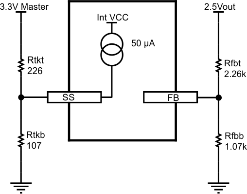 Figure 49. Tracking Option Input Detail
8.2.2.6 COUT Selection
None of the required COUT output capacitance is contained within the module. A minimum value ranging from 330 μF for 6-VOUT to 660 μF for 1.2-VOUT applications is required based on the values of internal compensation in the error amplifier. These minimum values can be decreased if the effective capacitor ESR is higher than 15 mΩ.
A Low ESR (15 mΩ) tantalum, organic semiconductor or specialty polymer capacitor types in parallel with a 47-nF X7R ceramic capacitor for high frequency noise reduction is recommended for obtaining lowest ripple. The output capacitor COUT may consist of several capacitors in parallel placed in close proximity to the module. The output voltage ripple of the module depends on the equivalent series resistance (ESR) of the capacitor bank, and can be calculated by multiplying the ripple current of the module by the effective impedance of your chosen output capacitors (for ripple current calculation, see Equation 15). Electrolytic capacitors will have large ESR and lead to larger output ripple than ceramic or polymer types. For this reason a combination of ceramic and polymer capacitors is recommended for low output ripple performance.
The output capacitor assembly must also meet the worst case ripple current rating of ΔiL, as calculated in Equation 15 below. Loop response verification is also valuable to confirm closed loop behavior.
For applications with dynamic load steps; Equation 8 provides a good first pass approximation of COUT for load transient requirements.

For 12 VIN, 3.3 VOUT, a transient voltage of 5% of VOUT = 0.165 V (ΔVOUT), a 9-A load step (ISTEP), an output capacitor effective ESR of 3 mΩ, and a switching frequency of 350 kHz (fSW):

NOTE
The stability requirement for minimum output capacitance must always be met.
One recommended output capacitor combination is two 330-μF, 15-mΩ ESR tantalum polymer capacitors connected in parallel with a 47-uF 6.3-V X5R ceramic. This combination provides excellent performance that may exceed the requirements of certain applications. Additionally some small 47-nF ceramic capacitors can be used for high-frequency EMI suppression.
8.2.2.7 CIN Selection
The LMZ13610 module contains two internal ceramic input capacitors. Additional input capacitance is required external to the module to handle the input ripple current of the application. The input capacitor can be several capacitors in parallel. This input capacitance must be located in very close proximity to the module. Input capacitor selection is generally directed to satisfy the input ripple current requirements rather than by capacitance value. Input ripple current rating is dictated by Equation 10:

where
- D ≊ VOUT / VIN
As a point of reference, the worst case ripple current will occur when the module is presented with full load current and when VIN = 2 × VOUT.
Recommended minimum input capacitance is 30-µF X7R (or X5R) ceramic with a voltage rating at least 25% higher than the maximum applied input voltage for the application. It is also recommended that attention be paid to the voltage and temperature derating of the capacitor selected.
NOTE
Ripple current rating of ceramic capacitors may be missing from the capacitor data sheet and you may have to contact the capacitor manufacturer for this parameter.
If the system design requires a certain minimum value of peak-to-peak input ripple voltage (ΔVIN) to be maintained then Equation 11 may be used.

If ΔVIN is 200 mV or 1.66% of VIN for a 12-V input to 3.3-V output application and fSW = 350 kHz then:

Additional bulk capacitance with higher ESR may be required to damp any resonant effects of the input capacitance and parasitic inductance of the incoming supply lines. The LMZ13610 typical applications schematic and evaluation board include a 150-μF 50-V aluminum capacitor for this function. There are many situations where this capacitor is not necessary.
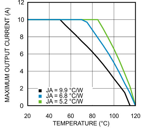
Another way to estimate the temperature rise of a design is using θJA. An estimate of θJA for varying heat sinking copper areas and airflows can be found in the Typical Characteristics. If our design required the same operating conditions as before but had 225 LFPM of airflow. We locate the required θJA of

On the θJA vs copper heatsinking curve, the copper area required for this application is now only 2 square inches. The airflow reduced the required heat sinking area by a factor of three.
To reduce the heat sinking copper area further, this package is compatible with D3-PAK surface mount heat sinks.
For an example of a high thermal performance PCB layout for SIMPLE SWITCHER power modules, refer to AN-2093 (SNVA460), AN-2084 (SNVA456), AN-2125 (SNVA473), AN-2020 (SNVA419) and AN-2026 (SNVA424).
8.2.2.8 Discontinuous Conduction and Continuous Conduction Modes Selection
The approximate formula for determining the DCM/CCM boundary is as follows:

The inductor internal to the module is 2.2 μH. This value was chosen as a good balance between low and high input voltage applications. The main parameter affected by the inductor is the amplitude of the inductor ripple current (ΔiL). ΔiL can be calculated with:

where
- VIN is the maximum input voltage
- fSW is typically 359 kHz
If the output current IOUT is determined by assuming that IOUT = IL, the higher and lower peak of ΔiL can be determined.
8.2.3 Application Curves
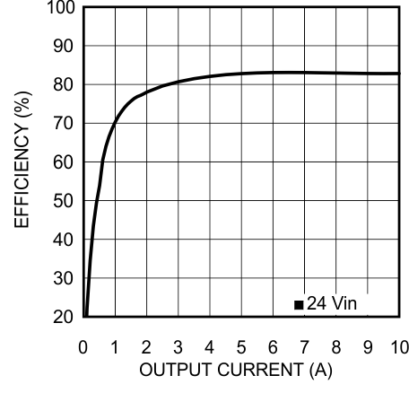
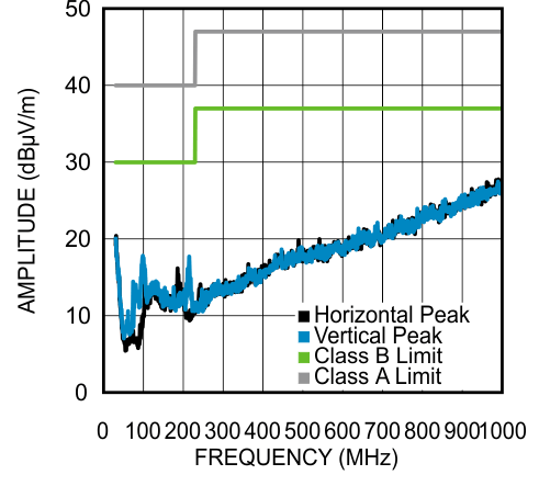
| VIN = 24 V, VOUT = 5 V, IOUT = 10 A |
