JAJSBZ7E JULY   2013  – December 2019 LMZ31710

PRODUCTION DATA.  

  1. 特長
  2. アプリケーション
  3. 概要
    1.     Device Images
      1.      アプリケーション概略図
  4. 改訂履歴
  5. Pin Configuration and Functions
    1.     Pin Functions
  6. Specifications
    1. 6.1 Absolute Maximum Ratings
    2. 6.2 ESD Ratings
    3. 6.3 Recommended Operating Conditions
    4. 6.4 Thermal Information
    5. 6.5 Electrical Characteristics
    6. 6.6 Typical Characteristics (PVIN = VIN = 12 V)
    7. 6.7 Typical Characteristics (PVIN = VIN = 5 V)
    8. 6.8 Typical Characteristics (PVIN = 3.3 V, VIN = 5 V)
  7. Detailed Description
    1. 7.1 Overview
    2. 7.2 Functional Block Diagram
    3. 7.3 Feature Description
      1. 7.3.1  VIN and PVIN Input Voltage
      2. 7.3.2  3.3-V PVIN Operation
      3. 7.3.3  Adjusting the Output Voltage (0.6 V to 5.5 V)
      4. 7.3.4  Capacitor Recommendations For the LMZ31710 Power Supply
        1. 7.3.4.1 Capacitor Technologies
          1. 7.3.4.1.1 Electrolytic, Polymer-Electrolytic Capacitors
          2. 7.3.4.1.2 Ceramic Capacitors
          3. 7.3.4.1.3 Tantalum, Polymer-Tantalum Capacitors
        2. 7.3.4.2 Input Capacitor
        3. 7.3.4.3 Output Capacitor
      5. 7.3.5  Transient Response
        1. 7.3.5.1 Transient Response Waveforms
      6. 7.3.6  Power Good (PWRGD)
      7. 7.3.7  Light Load Efficiency (LLE)
      8. 7.3.8  SYNC_OUT
      9. 7.3.9  Parallel Operation
      10. 7.3.10 Power-Up Characteristics
      11. 7.3.11 Pre-Biased Start-Up
      12. 7.3.12 Remote Sense
      13. 7.3.13 Thermal Shutdown
      14. 7.3.14 Output On/Off Inhibit (INH)
      15. 7.3.15 Slow Start (SS/TR)
      16. 7.3.16 Overcurrent Protection
      17. 7.3.17 Synchronization (CLK)
      18. 7.3.18 Sequencing (SS/TR)
    4. 7.4 Device Functional Modes
      1. 7.4.1 Programmable Undervoltage Lockout (UVLO)
  8. Application and Implementation
    1. 8.1 Application Information
    2. 8.2 Typical Application
      1. 8.2.1 Design Requirements
      2. 8.2.2 Detailed Design Procedure
        1. 8.2.2.1 Custom Design With WEBENCH® Tools
        2. 8.2.2.2 Setting The Output Voltage
        3. 8.2.2.3 Setting the Switching Frequency
        4. 8.2.2.4 Input Capacitance
        5. 8.2.2.5 Output Capacitance
    3. 8.3 Additional Application Schematics
  9. Power Supply Recommendations
  10. 10Layout
    1. 10.1 Layout Considerations
    2. 10.2 Layout Examples
      1. 10.2.1 EMI
  11. 11デバイスおよびドキュメントのサポート
    1. 11.1 デバイス・サポート
      1. 11.1.1 開発サポート
        1. 11.1.1.1 WEBENCH®ツールによるカスタム設計
      2. 11.1.2 デベロッパー・ネットワークの製品に関する免責事項
    2. 11.2 ドキュメントのサポート
      1. 11.2.1 関連資料
    3. 11.3 ドキュメントの更新通知を受け取る方法
    4. 11.4 サポート・リソース
    5. 11.5 商標
    6. 11.6 静電気放電に関する注意事項
    7. 11.7 Glossary
  12. 12メカニカル、パッケージ、および注文情報
    1. 12.1 Tape and Reel Information

パッケージ・オプション

メカニカル・データ(パッケージ|ピン)
サーマルパッド・メカニカル・データ
発注情報

Power-Up Characteristics

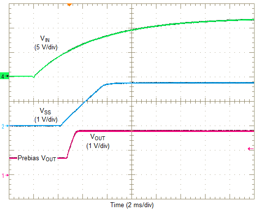
When configured as shown in the application circuit on page 1, the LMZ31710 produces a regulated output voltage following the application of a valid input voltage. During the power-up, internal soft-start circuitry slows the rate that the output voltage rises, thereby limiting the amount of in-rush current that can be drawn from the input source. Figure 24 shows the start-up waveforms for a LMZ31710, operating from a 5-V input (PVIN = VIN) and with the output voltage adjusted to 1.8 V. Figure 25 shows the start-up waveforms for a LMZ31710 starting up into a pre-biased output voltage. The waveforms were measured with a 5-A constant current load.
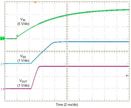
LMZ31710 start_up.pngFigure 24. Start-Up Waveforms
LMZ31710 prebias_start_up.pngFigure 25. Start-Up Into Pre-Bias