JAJSFF9B March 2016 – May 2018 TAS5751M
PRODUCTION DATA.
- 1 特長
- 2 アプリケーション
- 3 概要
- 4 改訂履歴
- 5 Pin Configuration and Functions
-
6 Specifications
- 6.1 Absolute Maximum Ratings
- 6.2 ESD Ratings
- 6.3 Recommended Operating Conditions
- 6.4 Thermal Characteristics
- 6.5 Electrical Characteristics
- 6.6 Speaker Amplifier Characteristics
- 6.7 Protection Characteristics
- 6.8 Master Clock Characteristics
- 6.9 I²C Interface Timing Requirements
- 6.10 Serial Audio Port Timing Requirements
- 6.11 Typical Characteristics
-
7 Detailed Description
- 7.1 Overview
- 7.2 Functional Block Diagram
- 7.3 Audio Signal Processing Overview
- 7.4 Feature Description
- 7.5 Device Functional Modes
- 7.6 Programming
- 7.7
Register Maps
- 7.7.1 Register Summary
- 7.7.2
Detailed Register Descriptions
- 7.7.2.1 Clock Control Register (0x00)
- 7.7.2.2 Device ID Register (0x01)
- 7.7.2.3 Error Status Register (0x02)
- 7.7.2.4 System Control Register 1 (0x03)
- 7.7.2.5 Serial Data Interface Register (0x04)
- 7.7.2.6 System Control Register 2 (0x05)
- 7.7.2.7 Soft Mute Register (0x06)
- 7.7.2.8 Volume Registers (0x07, 0x08, 0x09)
- 7.7.2.9 Volume Configuration Register (0x0E)
- 7.7.2.10 Modulation Limit Register (0x10)
- 7.7.2.11 Interchannel Delay Registers (0x11, 0x12, 0x13, and 0x14)
- 7.7.2.12 PWM Shutdown Group Register (0x19)
- 7.7.2.13 Start/Stop Period Register (0x1A)
- 7.7.2.14 Oscillator Trim Register (0x1B)
- 7.7.2.15 BKND_ERR Register (0x1C)
- 7.7.2.16 Input Multiplexer Register (0x20)
- 7.7.2.17 PWM Output MUX Register (0x25)
- 7.7.2.18 AGL Control Register (0x46)
- 7.7.2.19 PWM Switching Rate Control Register (0x4F)
- 7.7.2.20 Bank Switch and EQ Control (0x50)
-
8 Application and Implementation
- 8.1 Application Information
- 8.2
Typical Applications
- 8.2.1
Stereo Bridge Tied Load Application
- 8.2.1.1 Design Requirements
- 8.2.1.2 Detailed Design Procedure
- 8.2.1.3 Application Performance Plots
- 8.2.2 Mono Parallel Bridge Tied Load Application
- 8.2.1
Stereo Bridge Tied Load Application
- 9 Power Supply Recommendations
- 10Layout
- 11デバイスおよびドキュメントのサポート
- 12メカニカル、パッケージ、および注文情報
パッケージ・オプション
メカニカル・データ(パッケージ|ピン)
- DCA|48
サーマルパッド・メカニカル・データ
- DCA|48
発注情報
6.11.1 Typical Characteristics - Stereo BTL Mode
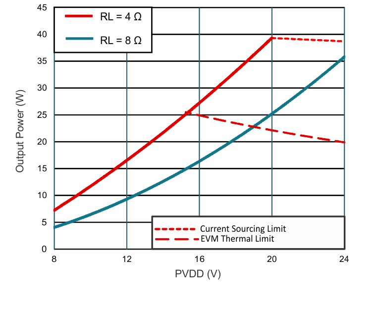 Figure 5. Output Power vs Supply Voltage
 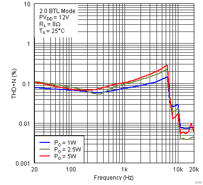 Figure 7. THD+N vs Frequency
 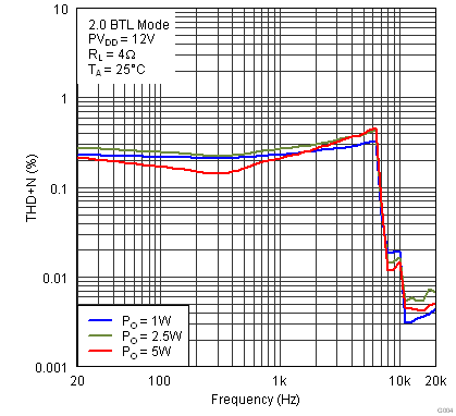 Figure 9. THD+N vs Frequency
 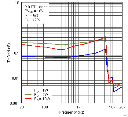 Figure 11. THD+N vs Frequency
 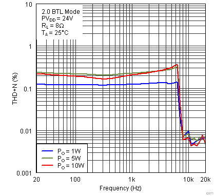 Figure 13. THD+N vs Frequency
 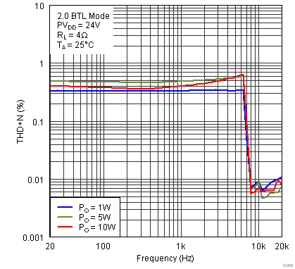 Figure 15. THD+N vs Frequency
 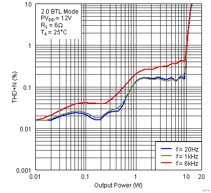 Figure 17. THD+N vs Output Power
 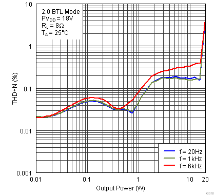 Figure 19. THD+N vs Output Power
 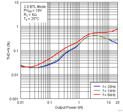 Figure 21. THD+N vs Output Power
 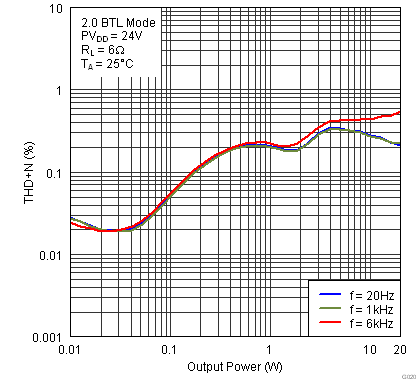 Figure 23. THD+N vs Output Power
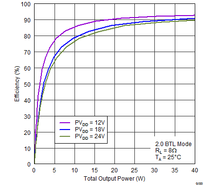
| Total Output Power includes power delivered from both amplifier outputs. For instance, 40 W of total output power means 2 × 20 W, with 20 W delivered by one channel and 20 W delivered by the other channel. |
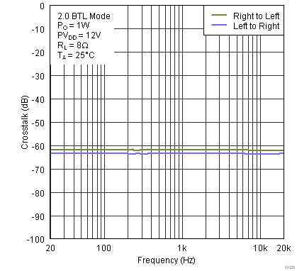 Figure 27. Crosstalk vs Frequency
 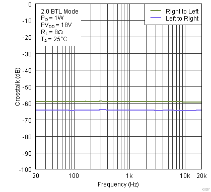 Figure 29. Crosstalk vs Frequency
 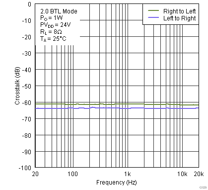 Figure 31. Crosstalk vs Frequency
 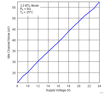 Figure 6. Idle Channel Noise vs Supply Voltage
 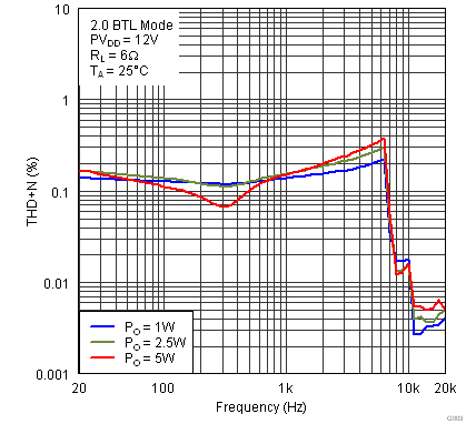 Figure 8. THD+N vs Frequency
 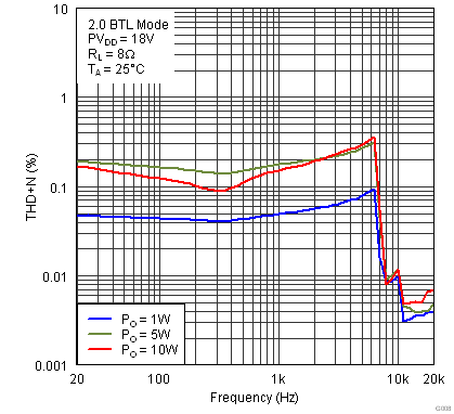 Figure 10. THD+N vs Frequency
 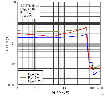 Figure 12. THD+N vs Frequency
 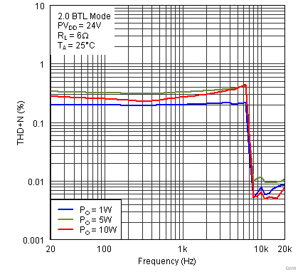 Figure 14. THD+N vs Frequency
 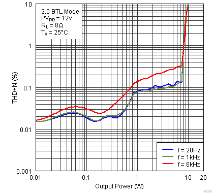 Figure 16. THD+N vs Output Power
 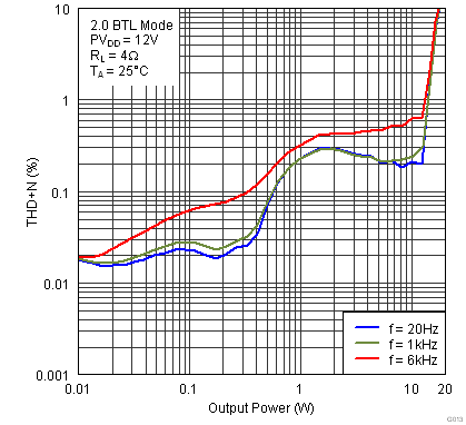 Figure 18. THD+N vs Output Power
 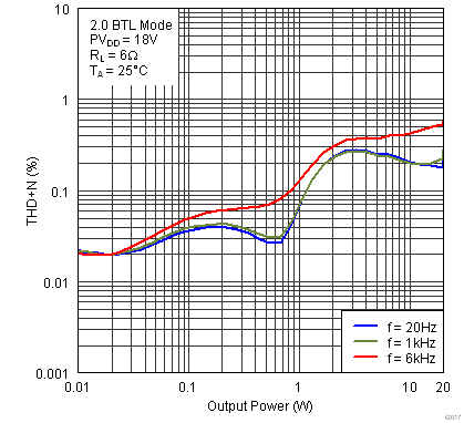 Figure 20. THD+N vs Output Power
 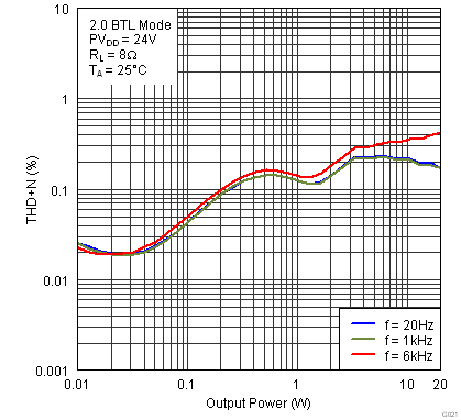 Figure 22. THD+N vs Output Power
 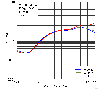 Figure 24. THD+N vs Output Power
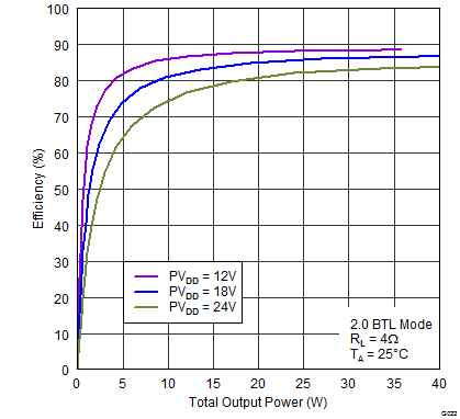
| Total Output Power includes power delivered from both amplifier outputs. For instance, 40 W of total output power means 2 × 20 W, with 20 W delivered by one channel and 20 W delivered by the other channel. |
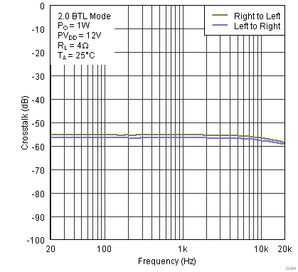 Figure 28. Crosstalk vs Frequency
 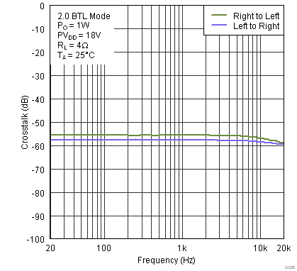 Figure 30. Crosstalk vs Frequency
 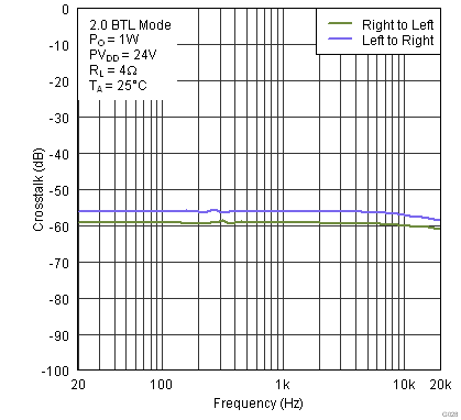 Figure 32. Crosstalk vs Frequency