JAJSHS9 August   2019 TMUX1247

PRODUCTION DATA.  

  1. 特長
  2. アプリケーション
  3. 概要
    1.     Device Images
      1.      アプリケーションの例
      2.      TMUX1247 のブロック図
  4. 改訂履歴
  5. Pin Configuration and Functions
    1.     Pin Functions
  6. Specifications
    1. 6.1 Absolute Maximum Ratings
    2. 6.2 ESD Ratings
    3. 6.3 Recommended Operating Conditions
    4. 6.4 Thermal Information
    5. 6.5 Electrical Characteristics (VDD = 5 V ±10 %), GND = 0 V unless otherwise specified.
    6. 6.6 Electrical Characteristics (VDD = 3.3 V ±10 %), GND = 0 V unless otherwise specified.
    7. 6.7 Electrical Characteristics (VDD = 1.8 V ±10 %), GND = 0 V unless otherwise specified.
    8. 6.8 Electrical Characteristics (VDD = 1.2 V ±10 %), GND = 0 V unless otherwise specified.
    9. 6.9 Typical Characteristics
  7. Parameter Measurement Information
    1. 7.1 On-Resistance
    2. 7.2 Off-Leakage Current
    3. 7.3 On-Leakage Current
    4. 7.4 Transition Time
    5. 7.5 Break-Before-Make
    6. 7.6 Charge Injection
    7. 7.7 Off Isolation
    8. 7.8 Crosstalk
    9. 7.9 Bandwidth
  8. Detailed Description
    1. 8.1 Overview
    2. 8.2 Functional Block Diagram
    3. 8.3 Feature Description
      1. 8.3.1 Bidirectional Operation
      2. 8.3.2 Rail to Rail Operation
      3. 8.3.3 1.8 V Logic Compatible Inputs
      4. 8.3.4 Fail-Safe Logic
    4. 8.4 Device Functional Modes
    5. 8.5 Truth Tables
  9. Application and Implementation
    1. 9.1 Application Information
    2. 9.2 Typical Application
      1. 9.2.1 Input Control for Power Amplifier
        1. 9.2.1.1 Design Requirements
        2. 9.2.1.2 Detailed Design Procedure
        3. 9.2.1.3 Application Curve
      2. 9.2.2 Switchable Operational Amplifier Gain Setting
        1. 9.2.2.1 Design Requirements
        2. 9.2.2.2 Detailed Design Procedure
        3. 9.2.2.3 Application Curve
  10. 10Power Supply Recommendations
  11. 11Layout
    1. 11.1 Layout Guidelines
      1. 11.1.1 Layout Information
    2. 11.2 Layout Example
  12. 12デバイスおよびドキュメントのサポート
    1. 12.1 ドキュメントのサポート
      1. 12.1.1 関連資料
    2. 12.2 ドキュメントの更新通知を受け取る方法
    3. 12.3 コミュニティ・リソース
    4. 12.4 商標
    5. 12.5 静電気放電に関する注意事項
    6. 12.6 Glossary
  13. 13メカニカル、パッケージ、および注文情報

パッケージ・オプション

メカニカル・データ(パッケージ|ピン)
サーマルパッド・メカニカル・データ
発注情報

Off-Leakage Current

Source leakage current is defined as the leakage current flowing into or out of the source pin when the switch is off. This current is denoted by the symbol IS(OFF).

The setup used to measure off-leakage current is shown in Figure 8.
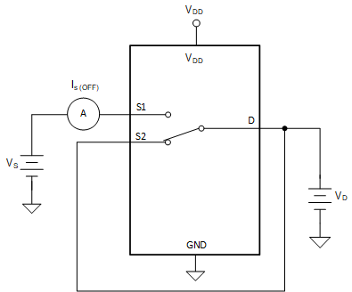
TMUX1247 Off_Leakage.gifFigure 8. Off-Leakage Measurement Setup