SLVS585E July 2005 – June 2015 TPS62110 , TPS62111 , TPS62112 , TPS62113
PRODUCTION DATA.
- 1 Features
- 2 Applications
- 3 Description
- 4 Typical Application Schematic
- 5 Revision History
- 6 Device Comparison Table
- 7 Pin Configuration and Functions
- 8 Specifications
- 9 Detailed Description
- 10Application and Implementation
- 11Power Supply Recommendations
- 12Layout
- 13Device and Documentation Support
- 14Mechanical, Packaging, and Orderable Information
パッケージ・オプション
メカニカル・データ(パッケージ|ピン)
- RSA|16
サーマルパッド・メカニカル・データ
- RSA|16
発注情報
1 Features
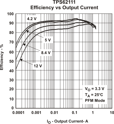
- High-Efficiency Synchronous Step-Down Converter With up to 95% Efficiency
- 3.1-V to 17-V Operating Input Voltage Range
- Adjustable Output Voltage Range: 1.2 V to 16 V
- Fixed Output Voltage Options Available in
3.3 V and 5 V - Synchronizable to External Clock: Up to 1.4 MHz
- Up to 1.5-A Output Current
- High Efficiency Over a Wide Load-Current
Range Due to PFM/PWM Operation Mode - 100% Maximum Duty Cycle for Lowest Dropout
- 20-µA Quiescent Current (Typical)
- Overtemperature and Overcurrent Protected
- Available in 16-Pin VQFN Package
2 Applications
- Point-of-Load Regulation From 12-V Buses
- Organizers, PDAs, and Handheld PCs
- Handheld Scanners
3 Description
The TPS6211x devices are a family of low-noise synchronous step-down DC-DC converters that are ideally suited for systems powered from a 2- to 4-cell Li-ion battery or from a 12-V or 15-V rail.
The TPS6211x devices are synchronous pulse width modulation (PWM) converters with integrated N- and P-channel power MOSFET switches. Synchronous rectification is used to increase efficiency and to reduce external component count. To achieve highest efficiency over a wide load-current range, the converter enters a power-saving, pulse frequency modulation (PFM) mode at light load currents. Operating frequency is typically 1 MHz, allowing the use of small inductor and capacitor values. The device can be synchronized to an external clock signal in the range of 0.8 MHz to 1.4 MHz. For low-noise operation, the converter can be operated in PWM-only mode. In shutdown mode, the current consumption is reduced to less than 2 µA. The TPS6211x family of devices are available in the 16-pin (RSA) VQFN package, and operate over a free-air temperature range of –40°C to 85°C.
Device Information(1)
| PART NUMBER | PACKAGE | BODY SIZE (NOM) |
|---|---|---|
| TPS62110 | VQFN (16) | 4.00 mm × 4.00 mm |
| TPS62111 | ||
| TPS62112 | ||
| TPS62113 |
- For all available packages, see the orderable addendum at the end of the data sheet.
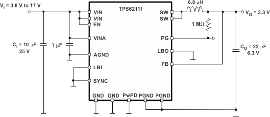
4 Typical Application Schematic

