SLUSCZ1 May 2017 TPS92518-Q1
PRODUCTION DATA.
- 1 Features
- 2 Applications
- 3 Description
- 4 Revision History
- 5 Pin Configuration and Functions
- 6 Specifications
- 7 Parameter Measurement Information
-
8 Detailed Description
- 8.1 Overview
- 8.2 Functional Block Diagram
- 8.3
Feature Description
- 8.3.1 General Operation
- 8.3.2 Important System Considerations: Off-Timer and Maximum Peak Threshold Values
- 8.3.3 Shunt FET or Matrix dimming: Maximum Off-timer Calculation
- 8.3.4 VIN and the VCC Internal Regulators
- 8.3.5 Output Enable Control Logic
- 8.3.6 BOOT Capacitor and BOOT UVLO
- 8.3.7 Drop-out Operation
- 8.3.8 Analog and PWM Dimming
- 8.3.9 VIN and CSPx Pin Configuration
- 8.3.10 Enable and Undervoltage Lock-out Configuration
- 8.3.11 Voltage Sampling and DAC Operation
- 8.3.12 Device Functional Modes
- 8.4 Serial Interface
- 8.5
Registers
- 8.5.1 CONTROL Register (Address = 00h) [reset = 00h]
- 8.5.2 STATUS (FAULT) Register (Address = 01h) [reset = 10h]
- 8.5.3 THERM_WARN_LMT Register (Address = 02h) [reset = 80h]
- 8.5.4 LED1_PKTH_DAC Register (Address = 03h) [reset = 80h]
- 8.5.5 LED2_PKTH_DAC Register (Address = 04h) [reset = 80h]
- 8.5.6 LED1_TOFF_DAC Register (Address = 05h) [reset = 80h]
- 8.5.7 LED2_TOFF_DAC Register (Address = 06h) [reset = 80h]
- 8.5.8 LED1_MAXOFF_DAC Register (Address = 07h) [reset = 80h]
- 8.5.9 LED2_MAXOFF_DAC Register (Address = 08h) [reset = 80h]
- 8.5.10 VTHERM Register (Address = 09h) [reset = 0h]
- 8.5.11 LED1_MOST_RECENT Register (Address = 0Ah) [reset = 0h]
- 8.5.12 LED1_LAST_ON Register (Address = 0Bh) [reset = 0h]
- 8.5.13 LED1_LAST_OFF Register (Address = 0Ch) [reset = 0h]
- 8.5.14 LED2_MOST_RECENT Register (Address = 0Dh) [reset = 0h]
- 8.5.15 LED2_LAST_ON Register (Address = 0Eh) [reset = 0h]
- 8.5.16 LED2_LAST_OFF Register (Address = 0Fh) [reset = 0h]
- 8.5.17 Reset Register (Address = 10h) [reset = 0h]
- 8.6 Programming
- 9 Application and Implementation
- 10Power Supply Recommendations
- 11Layout
- 12Device and Documentation Support
- 13Mechanical, Packaging, and Orderable Information
パッケージ・オプション
メカニカル・データ(パッケージ|ピン)
- PWP|24
サーマルパッド・メカニカル・データ
- PWP|24
発注情報
8.5.1 CONTROL Register (Address = 00h) [reset = 00h]
CONTROL is shown in Figure 38 and described in Table 3.
Return to Summary Table.
| 8 | 7 | 6 | 5 | 4 | 3 | 2 | 1 | 0 |
| RESERVED | THERM
SMPL EN |
VLED2
SMPL EN |
VLED1
SMPL EN |
LED2
EN |
LED1
EN |
|||
| R-0h | R/W-0h | R/W-0h | R/W-0h | R/W-0h | R/W-0h | |||
Table 3. CONTROL Register Field Descriptions
| Bit | Field | Type | Reset | Description |
|---|---|---|---|---|
| 8-5 | RESERVED | R | 0 |
Reserved |
| 4 | THERM_SMPL_EN | R/W | 0 |
Thermal sample enable 0 = Disable sampling 1 = Enable sampling |
| 3 | VLED2_SMPL_EN | R/W | 0 |
VLED2 sample enable 0 = Disable sampling 1 = Enable sampling |
| 2 | VLED1_SMPL_EN | R/W | 0 |
VLED1 sample enable 0 = Disable sampling 1 = Enable sampling |
| 1 | LED2_EN | R/W | 0 |
LED2 enable. This bit controls the operation state of channel 2. 0 = Disable LED channel 2 1 = Enable LED channel 2 |
| 0 | LED1_EN | R/W | 0 |
LED1 enable. This bit controls the operation state of channel 1. 0 = Disable LED channel 1 1 = Enable LED channel 1 |
xSMPL_EN: The TPS92518-Q1 Analog to Digital Converter (ADC) input is multiplexed between 3 inputs: the thermal sensor and the two output voltages. Each input is sampled consecutively. Sampling a single input increases the sampling frequency. For example: an ADC sample and conversion requires ~100us. If one item is selected it is sampled at roughly 10 kHz. If all three inputs are selected each is sampled at ~3.3 kHz.
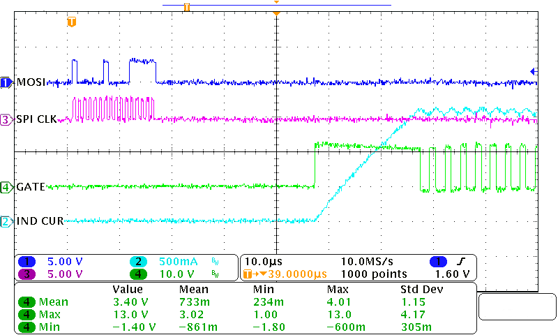
LEDx_EN: The TPS92518-Q1 PWMx pin AND the corresponding LEDxEN bit must be high for a channel to be enabled. If not using the external PWM input, tie the pin to VCC. The use of the LEDxEN register also enables the corresponding channel SWx pin internal pull-down to ensure no current flows to the LED load. A sample of the timing and waveforms around a SPI enable write are shown in Figure 39.
LEDxEN control may be bypassed using an analog activated override via the EN/UV pin. By applying a voltage >VEN/UV2 (23.6 V Typical) the contents of LEDxEN are ignored and the TPS92518-Q1 operates without SPI communication using the default register values. This is discussed in EN/UV2 - SPI Control Bypass
 Figure 39. SPI Enable Write Waveform Example