JAJSF50E December   2012  – April 2018 DRV2605

PRODUCTION DATA.  

  1. 特長
  2. アプリケーション
  3. 概要
  4. 改訂履歴
  5. Pin Configuration and Functions
    1.     Pin Functions
  6. Specifications
    1. 6.1 Absolute Maximum Ratings
    2. 6.2 ESD Ratings
    3. 6.3 Recommended Operating Conditions
    4. 6.4 Thermal Information
    5. 6.5 Electrical Characteristics
    6. 6.6 Timing Requirements
    7. 6.7 Switching Characteristics
    8. 6.8 Typical Characteristics
  7. Detailed Description
    1. 7.1 Overview
    2. 7.2 Functional Block Diagram
    3. 7.3 Feature Description
      1. 7.3.1  Support for ERM and LRA Actuators
      2. 7.3.2  Smart-Loop Architecture
        1. 7.3.2.1 Auto-Resonance Engine for LRA
        2. 7.3.2.2 Real-Time Resonance-Frequency Reporting for LRA
        3. 7.3.2.3 Automatic Overdrive and Braking
          1. 7.3.2.3.1 Startup Boost
          2. 7.3.2.3.2 Brake Factor
          3. 7.3.2.3.3 Brake Stabilizer
        4. 7.3.2.4 Automatic Level Calibration
          1. 7.3.2.4.1 Automatic Compensation for Resistive Losses
          2. 7.3.2.4.2 Automatic Back-EMF Normalization
          3. 7.3.2.4.3 Calibration Time Adjustment
          4. 7.3.2.4.4 Loop-Gain Control
          5. 7.3.2.4.5 Back-EMF Gain Control
        5. 7.3.2.5 Actuator Diagnostics
      3. 7.3.3  Open-Loop Operation for LRA
      4. 7.3.4  Open-Loop Operation for ERM
      5. 7.3.5  Flexible Front-End Interface
        1. 7.3.5.1 PWM Interface
        2. 7.3.5.2 Internal Memory Interface
          1. 7.3.5.2.1 Waveform Sequencer
          2. 7.3.5.2.2 Library Parameterization
        3. 7.3.5.3 Real-Time Playback (RTP) Interface
        4. 7.3.5.4 Analog Input Interface
        5. 7.3.5.5 Audio-to-Vibe Interface
        6. 7.3.5.6 Input Trigger Option
          1. 7.3.5.6.1 I2C Trigger
          2. 7.3.5.6.2 Edge Trigger
          3. 7.3.5.6.3 Level Trigger
      6. 7.3.6  Edge Rate Control
      7. 7.3.7  Constant Vibration Strength
      8. 7.3.8  Battery Voltage Reporting
      9. 7.3.9  One-Time Programmable (OTP) Memory for Configuration
      10. 7.3.10 Low-Power Standby
      11. 7.3.11 Device Protection
        1. 7.3.11.1 Thermal Protection
        2. 7.3.11.2 Overcurrent Protection of the Actuator
    4. 7.4 Device Functional Modes
      1. 7.4.1 Power States
        1. 7.4.1.1 Operation With VDD < 2.5 V (Minimum VDD)
        2. 7.4.1.2 Operation With VDD > 6 V (Absolute Maximum VDD)
        3. 7.4.1.3 Operation With EN Control
        4. 7.4.1.4 Operation With STANDBY Control
        5. 7.4.1.5 Operation With DEV_RESET Control
        6. 7.4.1.6 Operation in the Active State
      2. 7.4.2 Changing Modes of Operation
      3. 7.4.3 Operation of the GO Bit
      4. 7.4.4 Operation During Exceptional Conditions
        1. 7.4.4.1 Operation With No Actuator Attached
        2. 7.4.4.2 Operation With a Short at REG Pin
        3. 7.4.4.3 Operation With a Short at OUT+, OUT–, or Both
    5. 7.5 Programming
      1. 7.5.1 Auto-Resonance Engine Programming for the LRA
        1. 7.5.1.1 Drive-Time Programming
        2. 7.5.1.2 Current-Dissipation Time Programming
        3. 7.5.1.3 Blanking Time Programming
      2. 7.5.2 Automatic-Level Calibration Programming
        1. 7.5.2.1 Rated Voltage Programming
        2. 7.5.2.2 Overdrive Voltage-Clamp Programming
      3. 7.5.3 I2C Interface
        1. 7.5.3.1 TI Haptic Broadcast Mode
        2. 7.5.3.2 General I2C Operation
        3. 7.5.3.3 Single-Byte and Multiple-Byte Transfers
        4. 7.5.3.4 Single-Byte Write
        5. 7.5.3.5 Multiple-Byte Write and Incremental Multiple-Byte Write
        6. 7.5.3.6 Single-Byte Read
        7. 7.5.3.7 Multiple-Byte Read
      4. 7.5.4 Programming for Open-Loop Operation
        1. 7.5.4.1 Programming for ERM Open-Loop Operation
        2. 7.5.4.2 Programming for LRA Open-Loop Operation
      5. 7.5.5 Programming for Closed-Loop Operation
      6. 7.5.6 Auto Calibration Procedure
      7. 7.5.7 Programming On-Chip OTP Memory
      8. 7.5.8 Waveform Playback Programming
        1. 7.5.8.1 Data Formats for Waveform Playback
          1. 7.5.8.1.1 Open-Loop Mode
          2. 7.5.8.1.2 Closed-Loop Mode, Unidirectional
          3. 7.5.8.1.3 Closed-Loop Mode, Bidirectional
        2. 7.5.8.2 Waveform Setup and Playback
          1. 7.5.8.2.1 Waveform Playback Using RTP Mode
          2. 7.5.8.2.2 Waveform Playback Using the Analog-Input Mode
          3. 7.5.8.2.3 Waveform Playback Using PWM Mode
          4. 7.5.8.2.4 Waveform Playback Using Audio-to-Vibe Mode
          5. 7.5.8.2.5 Waveform Sequencer
          6. 7.5.8.2.6 Waveform Triggers
    6. 7.6 Register Map
      1. 7.6.1  Status (Address: 0x00)
        1. Table 4. Status Register Field Descriptions
      2. 7.6.2  Mode (Address: 0x01)
        1. Table 5. Mode Register Field Descriptions
      3. 7.6.3  Real-Time Playback Input (Address: 0x02)
        1. Table 6. Real-Time Playback Input Register Field Descriptions
      4. 7.6.4  (Address: 0x03)
        1. Table 7. Register Field Descriptions
      5. 7.6.5  Waveform Sequencer (Address: 0x04 to 0x0B)
        1. Table 8. Waveform Sequencer Register Field Descriptions
      6. 7.6.6  GO (Address: 0x0C)
        1. Table 9. GO Register Field Descriptions
      7. 7.6.7  Overdrive Time Offset (Address: 0x0D)
        1. Table 10. Overdrive Time Offset Register Field Descriptions
      8. 7.6.8  Sustain Time Offset, Positive (Address: 0x0E)
        1. Table 11. Sustain Time Offset, Positive Register Field Descriptions
      9. 7.6.9  Sustain Time Offset, Negative (Address: 0x0F)
        1. Table 12. Sustain Time Offset, Negative Register Field Descriptions
      10. 7.6.10 Brake Time Offset (Address: 0x10)
        1. Table 13. Brake Time Offset Register Field Descriptions
      11. 7.6.11 Audio-to-Vibe Control (Address: 0x11)
        1. Table 14. Audio-to-Vibe Control Register Field Descriptions
      12. 7.6.12 Audio-to-Vibe Minimum Input Level (Address: 0x12)
        1. Table 15. Audio-to-Vibe Minimum Input Level Register Field Descriptions
      13. 7.6.13 Audio-to-Vibe Maximum Input Level (Address: 0x13)
        1. Table 16. Audio-to-Vibe Maximum Input Level Register Field Descriptions
      14. 7.6.14 Audio-to-Vibe Minimum Output Drive (Address: 0x14)
        1. Table 17. Audio-to-Vibe Minimum Output Drive Register Field Descriptions
      15. 7.6.15 Audio-to-Vibe Maximum Output Drive (Address: 0x15)
        1. Table 18. Audio-to-Vibe Maximum Output Drive Register Field Descriptions
      16. 7.6.16 Rated Voltage (Address: 0x16)
        1. Table 19. Rated Voltage Register Field Descriptions
      17. 7.6.17 Overdrive Clamp Voltage (Address: 0x17)
        1. Table 20. Overdrive Clamp Voltage Register Field Descriptions
      18. 7.6.18 Auto-Calibration Compensation Result (Address: 0x18)
        1. Table 21. Auto-Calibration Compensation-Result Register Field Descriptions
      19. 7.6.19 Auto-Calibration Back-EMF Result (Address: 0x19)
        1. Table 22. Auto-Calibration Back-EMF Result Register Field Descriptions
      20. 7.6.20 Feedback Control (Address: 0x1A)
        1. Table 23. Feedback Control Register Field Descriptions
      21. 7.6.21 Control1 (Address: 0x1B)
        1. Table 24. Control1 Register Field Descriptions
      22. 7.6.22 Control2 (Address: 0x1C)
        1. Table 25. Control2 Register Field Descriptions
      23. 7.6.23 Control3 (Address: 0x1D)
        1. Table 26. Control3 Register Field Descriptions
      24. 7.6.24 Control4 (Address: 0x1E)
        1. Table 27. Control4 Register Field Descriptions
      25. 7.6.25 V(BAT) Voltage Monitor (Address: 0x21)
        1. Table 28. V(BAT) Voltage-Monitor Register Field Descriptions
      26. 7.6.26 LRA Resonance Period (Address: 0x22)
        1. Table 29. LRA Resonance-Period Register Field Descriptions
  8. Application and Implementation
    1. 8.1 Application Information
    2. 8.2 Typical Application
      1. 8.2.1 Design Requirements
      2. 8.2.2 Detailed Design Procedure
        1. 8.2.2.1 Actuator Selection
          1. 8.2.2.1.1 Eccentric Rotating-Mass Motors (ERM)
          2. 8.2.2.1.2 Linear Resonance Actuators (LRA)
            1. 8.2.2.1.2.1 Auto-Resonance Engine for LRA
        2. 8.2.2.2 Capacitor Selection
        3. 8.2.2.3 Interface Selection
        4. 8.2.2.4 Power Supply Selection
      3. 8.2.3 Application Curves
    3. 8.3 Initialization Setup
      1. 8.3.1 Initialization Procedure
      2. 8.3.2 Typical Usage Examples
        1. 8.3.2.1 Play a Waveform or Waveform Sequence from the ROM Waveform Memory
        2. 8.3.2.2 Play a Real-Time Playback (RTP) Waveform
        3. 8.3.2.3 Play a PWM or Analog Input Waveform
  9. Power Supply Recommendations
  10. 10Layout
    1. 10.1 Layout Guidelines
      1. 10.1.1 Trace Width
    2. 10.2 Layout Example
  11. 11デバイスおよびドキュメントのサポート
    1. 11.1 法的告知
    2. 11.2 波形ライブラリのエフェクト一覧
    3. 11.3 ドキュメントの更新通知を受け取る方法
    4. 11.4 コミュニティ・リソース
    5. 11.5 商標
    6. 11.6 静電気放電に関する注意事項
    7. 11.7 Glossary
  12. 12メカニカル、パッケージ、および注文情報

Level Trigger

The actions of the GO bit directly follow the IN/TRIG pin. When the IN/TRIG pin is high, the GO bit is high. When the IN/TRIG pin goes low, the GO bit clears. Therefore, a falling edge cancels the transaction. The level trigger can implement a GPIO-controlled buzz on-off controller if an appropriately long waveform is selected. The user must hold the IN/TRIG high for the entire duration of the waveform to complete the effect.
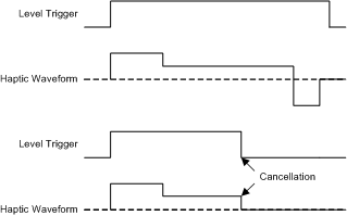
DRV2605 levelTrigger_slos854.gifFigure 14. Level Trigger Mode