JAJSQ80C september   2013  – october 2020 SN65DSI86

PRODUCTION DATA  

  1.   1
  2. 特長
  3. アプリケーション
  4. 概要
  5. Revision History
  6. Description (continued)
  7. Pin Configuration and Functions
  8. Specifications
    1. 7.1 Absolute Maximum Ratings
    2. 7.2 ESD Ratings
    3. 7.3 Recommended Operating Conditions
    4. 7.4 Thermal Information
    5. 7.5 Electrical Characteristics
    6. 7.6 Timing Requirements
    7. 7.7 Switching Characteristics
  9. Detailed Description
    1. 8.1 Overview
    2. 8.2 Functional Block Diagram
    3. 8.3 Feature Description
      1. 8.3.1 MIPI Dual DSI Interface
      2. 8.3.2 Embedded DisplayPort Interface
      3. 8.3.3 General-Purpose Input and Outputs
        1. 8.3.3.1 GPIO REFCLK and DSIA Clock Selection
        2. 8.3.3.2 Suspend Mode
        3. 8.3.3.3 Pulse Width Modulation (PWM)
    4. 8.4 Device Functional Modes
      1. 8.4.1 Reset Implementation
      2. 8.4.2 Power-Up Sequence
      3. 8.4.3 Power Down Sequence
      4. 8.4.4 Display Serial Interface (DSI)
        1. 8.4.4.1 DSI Lane Merging
        2. 8.4.4.2 DSI Supported Data Types
        3. 8.4.4.3 Generic Request Datatypes
          1. 8.4.4.3.1 Generic Read Request 2-Parameters Request
          2. 8.4.4.3.2 Generic Short Write 2-Parameters Request
          3. 8.4.4.3.3 Generic Long Write Packet Request
        4. 8.4.4.4 DSI Pixel Stream Packets
        5. 8.4.4.5 DSI Video Transmission Specifications
        6. 8.4.4.6 Video Format Parameters
        7. 8.4.4.7 GPU LP-TX Clock Requirements
      5. 8.4.5 DisplayPort
        1. 8.4.5.1  HPD (Hot Plug/Unplug Detection)
        2. 8.4.5.2  AUX_CH
          1. 8.4.5.2.1 Native Aux Transactions
        3. 8.4.5.3  I2C-Over-AUX
          1. 8.4.5.3.1 Direct Method (Clock Stretching)
          2. 8.4.5.3.2 Indirect Method (CFR Read/Write)
        4. 8.4.5.4  DisplayPort PLL
        5. 8.4.5.5  DP Output VOD and Pre-emphasis Settings
        6. 8.4.5.6  DP Main Link Configurability
        7. 8.4.5.7  DP Main Link Training
          1. 8.4.5.7.1 Manual Link Training
          2. 8.4.5.7.2 Fast Link Training
          3. 8.4.5.7.3 54
          4. 8.4.5.7.4 Semi-Auto Link Training
          5. 8.4.5.7.5 Redriver Semi-Auto Link Training
        8. 8.4.5.8  Panel Size vs DP Configuration
        9. 8.4.5.9  Panel Self Refresh (PSR)
        10. 8.4.5.10 Secondary Data Packet (SDP)
        11. 8.4.5.11 Color Bar Generator
        12. 8.4.5.12 DP Pattern
          1. 8.4.5.12.1 HBR2 Compliance Eye
          2. 8.4.5.12.2 80-Bit Custom Pattern
        13. 8.4.5.13 BPP Conversion
    5. 8.5 Programming
      1. 8.5.1 Local I2C Interface Overview
    6. 8.6 Register Map
      1. 8.6.1 Standard CFR Registers (PAGE 0)
  10. Application and Implementation
    1. 9.1 Application Information
    2. 9.2 Typical Application
      1. 9.2.1 1080p (1920x1080 60 Hz) Panel
        1. 9.2.1.1 Design Requirements
        2. 9.2.1.2 Detailed Design Procedure
          1. 9.2.1.2.1 eDP Design Procedure
          2. 9.2.1.2.2 76
          3. 9.2.1.2.3 DSI Design Procedure
          4. 9.2.1.2.4 78
          5. 9.2.1.2.5 Example Script
        3. 9.2.1.3 Application Curve
  11. 10Power Supply Recommendations
    1. 10.1 VCC Power Supply
    2. 10.2 VCCA Power supply
    3. 10.3 VPLL and VCCIO Power Supplies
  12. 11Layout
    1. 11.1 Layout Guidelines
      1. 11.1.1 DSI Guidelines
      2. 11.1.2 eDP Guidelines
      3. 11.1.3 Ground
    2. 11.2 Layout Example
  13. 12Device and Documentation Support
    1. 12.1 Documentation Support
      1. 12.1.1 Related Documentation
    2. 12.2 Receiving Notification of Documentation Updates
    3. 12.3 Community Resources
    4. 12.4 Trademarks
  14. 13Mechanical, Packaging, and Orderable Information

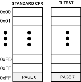
Register Map

Many of the SN65DSI86 functions are controlled by the Control and Status Registers (CSR). All CSR registers are accessible through the local I2C interface or through DSI interface.

Reads from reserved fields not described return zeros, and writes to read-only reserved registers are ignored. Writes to reserved register which are marked with W will produce unexpected behavior.

Table 8-18 Bit Field Access Tag Descriptions
ACCESS TAGNAMEMEANING
RReadThe field may be read by software
WWriteThe field may be written by software
SSetThe field may be set by a write of one. Writes of zeros to the field have no effect.
CClearThe field may be cleared by a write of one. Writes of zero to the field have no effect.
UUpdateHardware may autonomously update this field.
NANo AccessNot accessible or not applicable
GUID-E5362B93-4293-4B69-8444-31F08E4F09A6-low.gifFigure 8-14 Register Map