SNVAA67 March 2023 LM5012 , LM5012-Q1 , LM5013 , LM5013-Q1
5 48 VIN Design Example
This application note concludes with a typical design for LM5013-Q1, a 48 V to 12 V design. The LM5013-Q1 supports a load current up to 3 A. This design often requires the input to tolerate a VIN range of 36 V to 60 V. The following calculations are presented for the ramp injection circuit selection to minimize VOUT variation. Additionally, line and load regulation data is included, along with VOUT transient waveform in the case VIN falls below the designed minimum VIN of 36 V, resulting in the injected ripple falling out of device specification.
- The frequency is selected to be 300 kHz and the RRON resistor is calculated for the output voltage of 12 V.
- The corresponding feedback resistances are calculated for for the output voltage of 12 V and selected RFBT = 453 kΩ.
- The ramp capacitor (CA) can be calculated with the previously selected components.
- The ramp resistor (RA) is calculated for the minimum, input voltage (largest tON), and LM5013's minimum recommended ramp voltage of 12 mV.
- The ramp coupling cap (CB) is determined by the arbitrarily selected transient settling time of 50 us.
- The output capacitance of 44 μF is selected for typical load transient requirements which often supersedes the capacitance requirements for steady state/stability. A calculation wasn't necessarily followed.
- CIN and CBST are selected per the minimum LM5013-Q1 Automotive 100-V Input, 3.5-A Non-Synchronous Buck DC/DC Converter with Ultra-low IQ data sheet recommendation. DSW is selected to be a Schottky diode with a DC rating of 100 V and current rating of 3 A.
The load and line regulation data above was taken at VIN = 36 V, 42 V, 48 V, 54 V, and 60 V. The load current was varied from 0 A to 3 A.
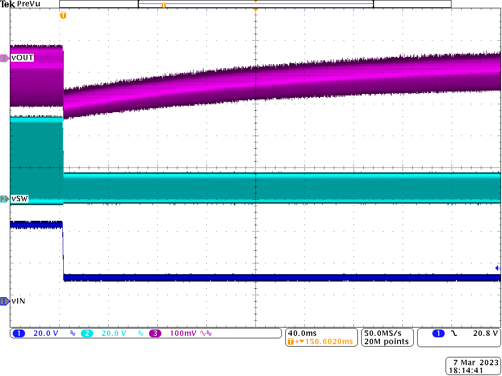
 Figure 5-3 Line Transient (48 V to 15 V),
Outside of Design Specification
Figure 5-3 Line Transient (48 V to 15 V),
Outside of Design SpecificationA line transient below the design's VIN range was applied and recorded was the VOUT transient. The converter matained regulation after the transient, with the net effect being reduced, peak-to-peak ripple and the DC output voltage falling. The ripple and DC output voltage fell as a result of the decreased inductor current ripple and average feedback voltage reducing, respectfully.
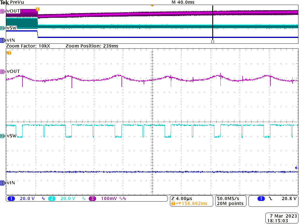
 Figure 5-4 Line Transient (48 V to 15 V),
Zoom-in of Double Pulsing on VSW as a Result of Insufficient Ramp
Injection
Figure 5-4 Line Transient (48 V to 15 V),
Zoom-in of Double Pulsing on VSW as a Result of Insufficient Ramp
InjectionA zoom-in of the VSW and VOUT was taken to highlight the effect of insufficient ramp injection. The injected ramp voltage falling much below 12 mV caused false triggering of PWM comparator used in the COT architecture. It can be seen that the switching behavior becomes less periodic as a result of the double pulses on VSW (small, then large).