SBOA198A July 2017 – March 2022 INA138 , INA139 , INA168 , INA169 , INA226
For high-side power supply current sensing needs, it is critical to understand the maximum voltage rating of the power supply. The maximum power supply voltage will drive the selection of a current sense amplifier. The common mode voltage of the current sense amplifier should exceed the maximum voltage on the power supply. For example, if a current is measured on the 48 V power supply with a transient voltage not exceeding 96 V a current sense amplifier with a maximum common mode voltage supporting 96 V needs to be designed. Likewise for a 400 V supply a common mode voltage of current sense amplifier supporting 400 V needs to be chosen.
The system cost solution of high voltage, high-side current sensing can be expensive considering a goal of <1% accuracy needs to be achieved. For common mode voltages higher than 90 V often the selection of current sense amplifiers are limited to isolation technology which can be expensive and BOM extensive. Below are some of the techniques that illustrates the extension of low voltage common mode current sense amplifiers beyond its maximum rating by adding a few inexpensive external components like resistors, diodes and PMOS FETs.
Common Mode Voltage Divider Using Resistors.
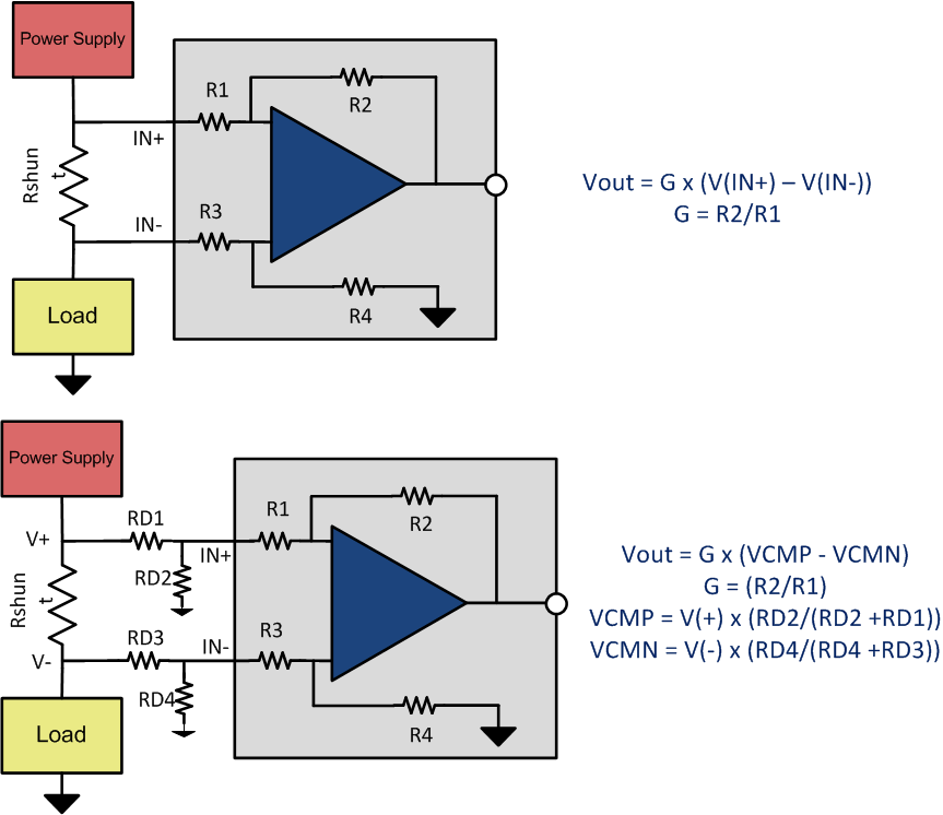
The simplest approach to monitor high voltage high-side current sensing is a design with a low voltage current sensing amplifier with external input voltage dividers, for example, if a 40 V common mode voltage amplifier is selected for a 80 V application, the 80 V input common mode needs to be divided down to 40 V common mode voltage. This voltage division can be accomplished using external resistor dividers as shown in the Figure 1-1. This is a simple design approach and the tradeoffs are significant. The gain error and CMRR of the amplifier are dependent on the accuracy and the matching of the external input divider resistors. Apart from gain error and CMRR errors, the tolerance of the external resistors will contribute to imbalance in input voltage causing additional output error. This error does increase over temperature depending on the drift specifications of the resistors. One technique to minimize output error is to use precision 0.1% matched low temperature drift external resistor dividers.
 Figure 1-1 Extending Common Mode Range
using Resistor Dividers
Figure 1-1 Extending Common Mode Range
using Resistor DividersExtending Common Mode Range for Current Output Amplifiers
As voltage dividers has serious
consequences with output error and degradation in performance, another alternative
approach is to shift the ground reference of the current output amplifier to the
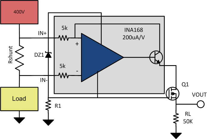
high voltage common mode node as shown in Figure 1-2.
Figure 1-2 enables current sensing at higher voltages beyond rated common mode voltage of
INA168 is 60V. This technique can be extended to any voltage beyond 60V by designing
an appropriate PMOS FET (Q1).
In Figure 1-2 Zener diode DZ1 regulates the supply voltage that the current shunt monitor operates within, and this voltage floats relative to the supply voltage. DZ1 is chosen to provide sufficient operating voltage for the combination of IC1 and Q1 over the expected power-supply range (typically from 5.1 V to 56 V). Select R1 to set the bias current for DZ1 at some value greater than the maximum quiescent current of IC1. The INA168 shown in Figure 1-2 is specified at 90 µA maximum at 400 V. The bias current in DZ1 is approximately 1 mA at 400 V, well in excess of IC1’s maximum current (the bias current value was selected to limit dissipation in R1 to less than 0.1 W). Connect a P-channel MOSFET, Q1, as shown to cascode the output current of IC1 down to or below ground level. Transistor Q1’s voltage rating should exceed the difference between the total supply and DZ1 by several volts because of the upward voltage swing on Q1’s source. Select RL, IC1’s load resistor, as if IC1 were used alone. The cascode connection of Q1 enables using IC1 well in excess of its normal 60-V rating. The example circuit shown in Figure 1-2 was specifically designed to operate at 400 V.
 Figure 1-2 High-Side DC Current
Measurements for 400-V Systems
Figure 1-2 High-Side DC Current
Measurements for 400-V SystemsExtending Common Mode Voltage Range for Power Monitors
System optimization and power monitoring for high voltage systems (40 V to 400 V), if implemented accurately can result in improvement of overall system power management and efficiency. Current, voltage and system power information can be beneficial in taking preventive steps to diagnose faults or calculate total power consumption of the system. Monitoring faults and power optimization will assist high voltage system in premature failures and significantly lower power savings by optimizing system shut down and wake up.
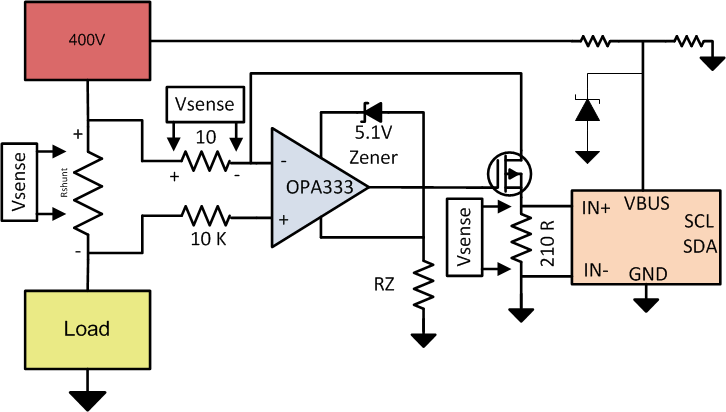
Figure 1-3 illustrates a methodology by using INA226 a 36 V common mode voltage power monitoring device to be used in applications supporting 40 V to 400 V systems. Shown in Figure 1-2 is the precision, rail-to-rail op amp OPA333 used to mirror the sense voltage across the shunt resistor on to a precision resistor R1. OPA333 is floated up to 400 V using a 5.1 V zener diode between its supply pins. The op amp drives the gate of the 600 V P-FET in a current follower configuration. A low leakage P-FET is chosen to obtain accurate readings even at the low end of the measurement. The voltage across R1 sets the drain current of the FET and by matching the resistor R2 in the drain of the FET to be equal to R1, VSENSE voltage is developed across R2 (VR2). Inputs of the current monitor INA226 are connected across R2 for current sensing. Hence the current monitor does not need the high common mode capability as it will only see common mode voltages around VSENSE which is usually less than 100mV. INA226 was chosen for current, voltage and power monitoring as it is a high accuracy current/voltage/power monitor with an I2C interface. The INA226 can also sense bus voltages less than 36 V. Since the bus voltage employed here is 400 V, a divider is employed to scale down the high voltage bus to a voltage within the common mode range of INA226. In this case a ratio of 64 is chosen and hence the bus voltage LSB can be scaled accordingly to obtain the actual bus voltage reading. In this case the a modified LSB of 80 mV could be used. Precision resistors are chosen for the divider to maintain accuracy of the bus measurement.
 Figure 1-3 High Voltage Power
Monitoring
Figure 1-3 High Voltage Power
Monitoring| Device | Optimized Parameter | Performance Trade-Off |
|---|---|---|
| LMP8645HV | Bandwidth : 900kHz, Package: SOT-23-6 | Slew rate: 0.5V/uS |
| INA220 | MSOP-8 Package, I2C interface, Selectable I2C address | Gain Error (1%), Shunt Offset Voltage: 100uV |
| INA139 | Package: SOT-23, Bandwidth: 4400 kHz, cost | Offset voltage: 1mV |