SLLA606 February 2023 ADS7038-Q1 , SN74HCS165-Q1 , TCA9539-Q1 , TIC12400-Q1 , TMUX1308-Q1
Current trends in automotive are moving towards consolidated designs by using zonal architectures to distribute power using semiconductor designs. This shift provides benefits such as optimized cabling between ECUs, increased software control, and zonal power distribution. By combining power distribution to more loads, sensors, and actuators into zonal modules, challenges for interfacing more inputs and outputs to a single automotive microcontroller (MCU), microprocessor, or system on a chip (SoC) become more prevalent.
The motivation for this article is to introduce methods of input-output (IO) expansion for inputs and outputs. The article discusses the key points of consideration for IO expansion including signal latency from the MCU to the IO interfacing device, software overhead, design size, and device features such as, autonomous monitoring, interrupt pin, wetting current, and type of interface; that is, general-purpose IO (GPIO), serial peripheral interface (SPI), inter-integrated circuit (I2C).
Input Expansion for Switches and Sensors
Examples of inputs typically used in zonal modules include: discrete high-voltage switches (active high, active low, push pull), discrete high-voltage signals from other control modules, resistor-coded switches, matrix switches, and analog sensors. There are 6 possible hardware designs for handling inputs and providing relief to the MCU:
- Shift Register
- Multiplexer (MUX)
- Analog-to-Digital Converter (ADC)
- IO Expander
- Multi-Switch Detection Interface (MSDI)
- Supporting MCU
This document considers 24 switch or sensor inputs that are needed in the application as an example. The inputs are either switches to battery, switches to ground, tri-state switches, or analog sensors. Some devices can only recognize a high or low discrete state and thus, cannot accommodate a tri-state switch or analog sensor. For these specific inputs the output of the IO expanding device must interface with an ADC pin on the MCU or the IO expanding device must have an integrated ADC. Depending on the type of switch a pullup or pulldown resistor (or both) is needed to keep the switch in a known state. An additional voltage divider can also be required to reduce the input voltage seen by the IO expanding device. Furthermore, reverse voltage protection, short-to-battery or short-to-ground protection can also be required in the system. If wetting current is required, an additional Discrete Wetting Current Circuit is needed or the IO expanding device has integrated wetting current.
Output Expansion for Load Drivers
Each zonal module can have a large number of load drivers to control the loads in the system. Typically, most of the load drivers are high-side switches and these are often controlled with GPIO from the system MCU. However, the MCU can have limited GPIO available to interface with all high-side switches and other circuits within the system. In the case of SPI-based high-side switches, IO expansion is needed to handle the large number of chip selects (CS). There are two possible hardware designs for handling high-side switches and providing relief to the MCU:
- IO Expander
- Supporting MCU
The rest of this brief analyzes each hardware IO design.
Shift Register
Shift registers are best to use when available GPIO are limited, less functionality is needed and minimal software overhead is preferred. Shift registers only require 4 GPIO from the MCU and provide the ability to daisy chain devices to output data into a single GPIO data output. The other 3 GPIO are used to drive CLK, SH/LD, and SER. By configuring the shift registers in a daisy chain, the number of interfacing GPIO is always four, making this design incredibly flexible for add-ons farther into the design process. However, while daisy chaining is a great design, the more shift registers that are daisy chained, the more latency increases. In terms of software overhead, the shift register only needs to have a CLK, SH/LD, and SER signal applied, but the data output needs to be polled periodically for status changes. This polling process influences the amount of software overhead needed. For a more detailed read on shift registers, see the Designing with Shift Registers application note.
The TI proposal in Figure 1 shows a design using 3 x SN74HCS165-Q1, which is an 8-channel shift register. The shift registers are shown in a daisy-chain implementation, reducing 24 switch inputs to 4 MCU GPIO.
Multiplexer (MUX)
A MUX is best to use when a pure analog design with minimal software overhead is needed, MCU wakeup is not required and only switch monitoring is needed, or the injection current control feature is preferred. In a typical zonal application, the MCU needs to regularly cycle the MUX truth table using A0, A1, and A2 to check the inputs for value changes. This determines the overall latency and software overhead. For information of timing characteristics of the MUX, there is a dedicated TI E2E FAQ which discusses MUX latency in detail.
The TI proposal in Figure 1-2 shows a design using 3 × TMUX1308-Q1, which is an 8-channel MUX. The design takes 24 switch inputs and requires a maximum of 15 GPIO on the MCU. This number can be reduced to 7 GPIO by connecting all EN pins together, A0 pins together, A1 pins together, and A2 pins together. By doing so, 4 GPIO are needed to control EN, A0, A1, A2, and 3 GPIO are required for receiving data from the MUX.
IO Expander
The IO expander is best to use when an I2C interface is preferred, and an interrupt pin is needed. For software overhead, configure the IO ports as inputs or outputs and then a register read is required to determine the value of the inputs and a register write is required to set the value of the outputs. For switch inputs, the IO expander can either poll the inputs or use the interrupt pin to check the inputs when flagged. With regards to signal latency, the IO expander devices are I2C target devices that can run at fast I2C bus (400 kHz). The latency is dependent on the I2C operating frequency and the bus loading conditions.
The TI proposal in Figure 3 uses 1 x TCA9539-Q1 (16-channel) and 1 x TCA6408-Q1 (8-channel) to take 24 inputs to a shared I2C bus.
The IO expander is also a great option for output expansion because I2C can be used to control the high-side switches greatly reducing the number of GPIO required. Configure the IO ports as inputs and outputs to interface with corresponding high-side switch pins.
Figure 4 shows how to use a GPIO expander to control high-side switches. If the current sense pin is needed for the high-side switches, the current sense pins can connect directly to an ADC pin on the MCU, or connect through a MUX (that is, TMUX1308-Q1) to an ADC pin on the MCU, or connect to an external ADC.
Analog-to-Digital Converter (ADC)
An ADC is best to use when SPI is required, there are more analog inputs than ADC pin availability within the MCU, and autonomous monitoring with an interrupt pin is required. Some software overhead is required to setup SPI communication and configure the registers. Considering latency, the ADS7038-Q1 is a successive-approximation (SAR) ADC that has different configuration modes. Depending on the configuration mode, the ADC can have zero latency (using In-The-Fly mode) to 2-cycle latency when using Manual mode. Overall, latency depends heavily on device application, sampling rate, and mode configuration of the device.
Figure 5 illustrates a design using 3 × ADS7038-Q1, which is an 8-channel ADC, to convert 24 inputs into SPI.
Multi-Switch Detection Interface (MSDI)
MSDI is best to use when SPI, integrated wetting current, high-voltage protection, and autonomous monitoring is needed. Some software overhead is required to configure the SPI communication and set the registers needed.
The latency of the signal can refer to the time between a state change of a switch and the time the interrupt signal is generated. This time can change based on the device configuration. The TIC12400-Q1, which is a 24-channel MSDI device, samples the inputs pins sequentially in a polling loop. The frequency of this loop can be configured to execute once every 2 ms to once every 4096 ms through the POLL_TIME register. The latency depends on where the switch transition occurs relative to the internal polling loop because these are asynchronous. Therefore, the latency is almost instantaneous, or almost the entire poll time. Other factors such as how the wetting current is applied (continuous or polling mode), the type of measurement (comparator or ADC), the number of input channels configured, the amount of time the wetting current is actively applied if in polling mode, and so forth, has an impact on latency.
The TI design in Figure 6 uses 1 x TIC12400-Q1 (24-channel) to reduce 24 inputs to an SPI. Since the wetting current is integrated into the device, some passive components are eliminated in comparison to other designs.
Supporting Microcontroller
Supporting microcontrollers are best to use when processing bandwidth on the primary processor is limited or dedicated towards certain functions. This provides increased flexibility as GPIO, SPI, and I2C pins are available for capturing signals, as well as transmitting data to the primary processor. Software overhead is more demanding compared to other designs described in this application brief; however, once communication with the primary processor is configured, there is more flexibility with communication preferences and local processing can be completed before the final data is sent to the primary host processor. The data can be sent out via GPIO, SPI, or I2C to the main processor, making the supporting MCU the most flexible design presented.
The TI design in Figure 7 uses a supporting MCU to accommodate 24 inputs to be processed locally, with the final data being sent to the primary host processor via GPIO, SPI, or I2C. A supporting MCU can also be used for output expansion with high-side switches. Overall, a supporting MCU works as a competitive design for IO expansion which is easily configurable.
Discrete Wetting Current Circuit
Different IO expansion hardware designs were discussed in the previous sections. This final section details a discrete wetting current circuit. Wetting current is the minimum amount of DC current needed to keep a mechanical switch in good health and is used to remove the excessive corrosion that can build up on a mechanical switch. If there is not enough wetting current applied, the switch can build up excessive resistance causing the switch to malfunction. Typically, wetting current is between 1 to 20 mA.
If the previously-listed devices do not offer integrated wetting current, then a discrete circuit is required. The circuit consists of two bi-polar junction transistors (BJT), resistors, and capacitors. A simulation was created to show example values for the discrete circuit. Depending on the type of switch, there are different configurations for a discrete wetting circuit.
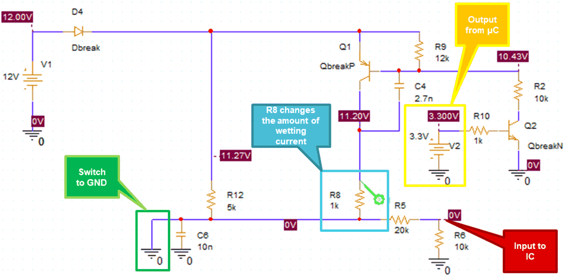
Figure 8 shows the schematic for a wetting circuit with switches to ground. Connect the gate of the second BJT (Q2) to a GPIO on the MCU. This GPIO turns the wetting current on or off as needed. R5 and R6 represent the voltage divider before the input switch is connected to the IO expanding device. The value of R8 changes the value of the wetting current. By setting R8 to 1 kΩ the wetting current simulated is 11 mA. The battery voltage also changes the value of the wetting current. If the battery voltage fluctuates up and down, then the wetting current also fluctuates up and down.
 Figure 1-8 Wetting Circuit for Switches to Ground
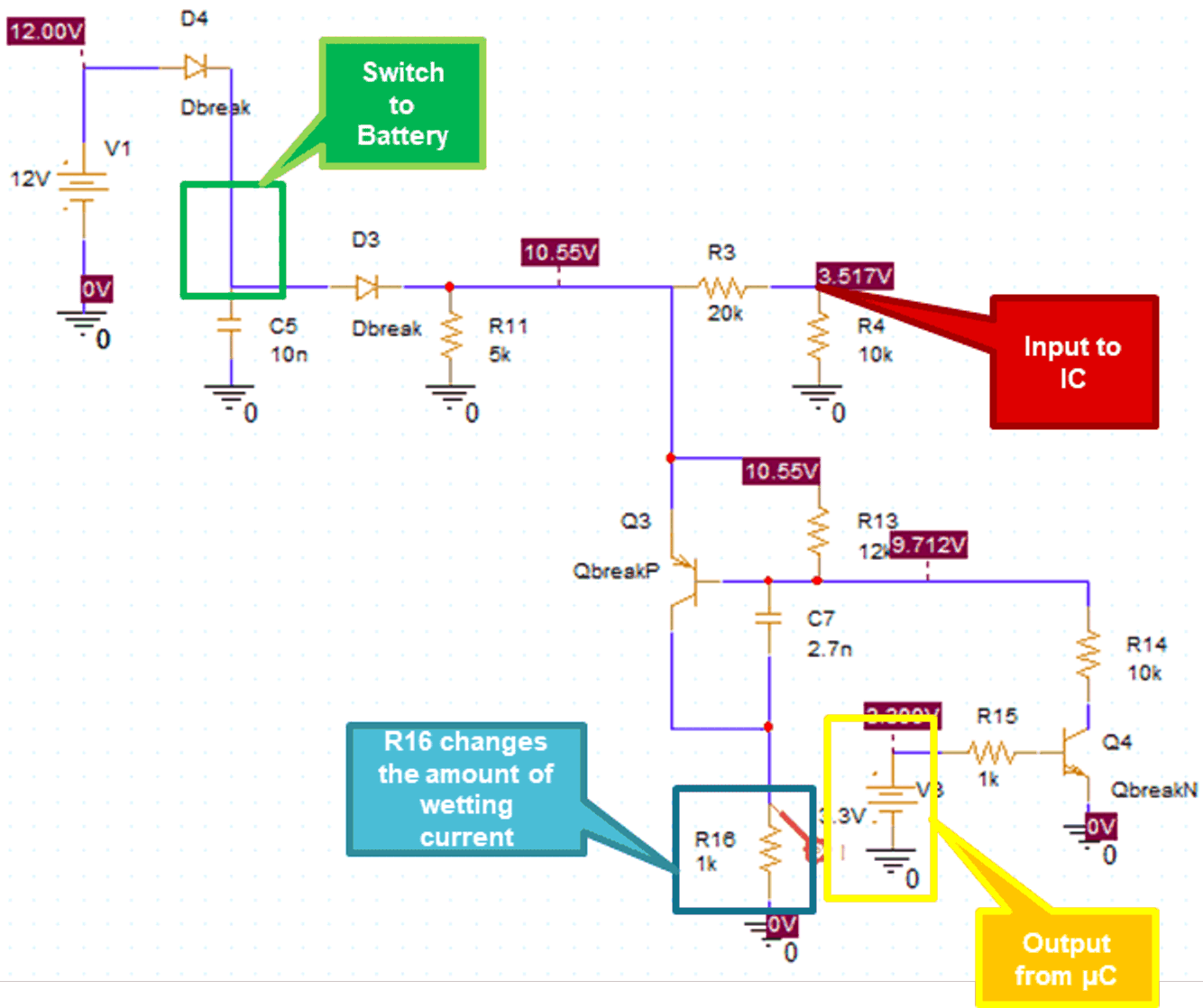
Figure 9 shows the schematic for a wetting circuit with switches to battery. Connect the gate of the second BJT (Q4) to a GPIO on the MCU. This GPIO turns the wetting current on or off as needed. R3 and R4 represent the voltage divider before the input switch is connected to the IO expanding device. In this circuit, R16 controls the value of the wetting current. By setting R16 to 1 kΩ, the simulated wetting current is 10.5 mA. The battery voltage impacts the value of the wetting current in this circuit as well.
 Figure 1-9 Wetting Circuit for Switches to Battery
Summary
This document presents methods of IO expansion for switch inputs and outputs using TI devices. The six possible hardware designs for input expansion are shift register, MUX, ADC, IO expander, MSDI, and a supporting MCU. For zonal modules that implement a large amount of high-side switches, an IO expander is an effective method to reduce the amount MCU GPIO required to control high-side switches.
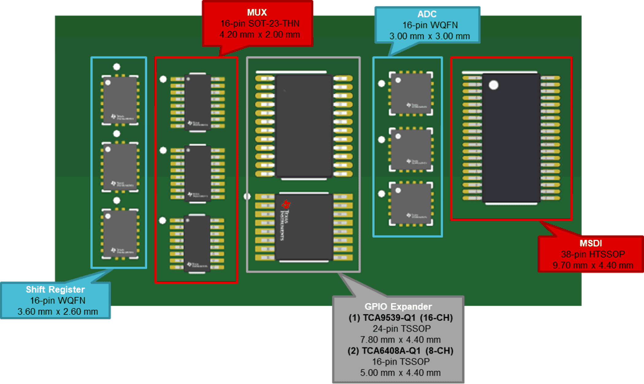
Figure 10 shows a comparison of the smallest packages for each input expanding hardware design. If a discrete wetting circuit is needed, that adds additional passive components to consider in the system board space.
 Figure 1-10 Package Size Comparison
The hardware designs were compared for latency, software overhead, design size, and device features such as, autonomous monitoring, interrupt pin, wetting current, and type of interface (that is, GPIO, SPI, I2C). Table 1 provides an overview of these key features needed to help engineers make the best selection for input expansion.
| Type | Device | Channels | Interface | Latency | Software Overhead | Interrupt | Autonomous Monitoring | Wetting Current |
|---|---|---|---|---|---|---|---|---|
Shift Register | SN74HCS165-Q1 | 8 | GPIO | Polling time, daisy chaining, and clock speed | Polling | No | No | Discrete |
MUX | TMUX1308-Q1 | 8 | GPIO | Polling time | Polling | No | No | Discrete |
IO Expander | TCA9539-Q1 TCA6408-Q1 | 8 or 16 | I2C | Clock speed and bus loading | I2C to configure a few registers | Yes | No | Discrete |
ADC | ADS7038-Q1 | 8 | SPI | Configuration and clock speed | SPI to configure many registers | Yes | Yes | Discrete |
MSDI | TIC12400-Q1 | 24 | SPI | Configuration and clock speed | SPI to configure many registers | Yes | Yes | Integrated |