SNVS323I December 2004 – February 2016 LP38690-ADJ , LP38692-ADJ
PRODUCTION DATA.
- 1 Features
- 2 Applications
- 3 Description
- 4 Revision History
- 5 Pin Configuration and Functions
- 6 Specifications
- 7 Detailed Description
-
8 Application and Implementation
- 8.1 Application Information
- 8.2 Typical Application
- 9 Power Supply Recommendations
- 10Layout
- 11Device and Documentation Support
- 12Mechanical, Packaging, and Orderable Information
Package Options
Mechanical Data (Package|Pins)
Thermal pad, mechanical data (Package|Pins)
Orderable Information
1 Features
- Input Voltage Range: 2.7 V to 10 V
- Output Voltage Range: 1.25 V to 9 V
- 2.5% Adjust Pin Voltage Accuracy (25°C)
- Low Dropout Voltage: 450 mV at 1 A (5-V Typical VOUT)
- Precision (Trimmed) Bandgap Reference
- Ensured Specs for –40°C to +125°C
- 1-µA Off-State Quiescent Current
- Thermal Overload Protection
- Foldback Current Limiting
- Enable (EN) Pin (LP38692-ADJ)
- 5-Pin SOT-223 and 6-Pin WSON Packages
3 Description
The LP38690-ADJ and LP38692-ADJ low dropout CMOS linear regulators provide 2.5% precision reference voltage, extremely low dropout voltage (450 mV at 1-A load current, VOUT = 5 V) and excellent AC performance utilizing ultralow equivalent series resistance (ESR) ceramic output capacitors.
The low thermal resistance of the WSON and SOT-223 packages allow the full operating current to be used even in high ambient temperature environments.
The use of a PMOS power transistor means that no DC base drive current is required to bias it allowing ground pin current to remain below 100 µA regardless of load current, input voltage, or operating temperature.
- Dropout Voltage: 450 mV (typical) at 1 A (typical 5-V out)
- Ground Pin Current: 55 µA (typical) at full load
- Adjust Pin Voltage: 2.5% (25°C) accuracy
Device Information(1)
| PART NUMBER | PACKAGE | BODY SIZE (NOM) |
|---|---|---|
| LP38690-ADJ | WSON (6) | 3.00 mm × 3.00 mm |
| LP38692-ADJ | ||
| LP38692-ADJ | SOT-223 (5) | 6.50 mm × 3.56 mm |
- For all available packages, see the orderable addendum at the end of the data sheet.
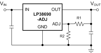
Simplified Schematic LP38690-ADJ

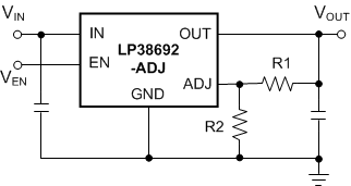
Simplified Schematic LP38692-ADJ
