SNVS481M November 2006 – December 2015 LP3910
PRODUCTION DATA.
- 1 Features
- 2 Applications
- 3 Description
- 4 Revision History
- 5 Device Comparison Tables
- 6 Pin Configuration and Functions
-
7 Specifications
- 7.1 Absolute Maximum Ratings
- 7.2 ESD Ratings
- 7.3 Recommended Operating Conditions
- 7.4 Thermal Information
- 7.5 Electrical Characteristics
- 7.6 Electrical Characteristics: I2C Interface
- 7.7 Electrical Characteristics: Li-Ion Battery Charger
- 7.8 Detection and Timing
- 7.9 Output Electrical Characteristics: CHG, STAT
- 7.10 Output Electrical Characteristics: NRST, IRQB, ONSTAT
- 7.11 Input Electrical Characteristics: USBSUSP, USBISEL
- 7.12 Input Electrical Characteristics: POWERACK, ONOFF, LDO2EN, BUCK1EN
- 7.13 Electrical Characteristics: LDO1 Low Dropout Linear Regulators
- 7.14 Electrical Characteristics: LDO2 Low Dropout Linear Regulator
- 7.15 Electrical Characteristics: Buck1 Converter
- 7.16 Electrical Characteristics: Buck2 Converter
- 7.17 Electrical Characteristics: Buck-Boost
- 7.18 Electrical Characteristics: ADC
- 7.19 I2C Timing Requirements
- 7.20 USB Timing Requirements
- 7.21 Typical Characteristics
-
8 Detailed Description
- 8.1 Overview
- 8.2 Functional Block Diagram
- 8.3
Feature Description
- 8.3.1 Buck1, Buck2: Synchronous Step-Down Magnetic DC-DC Converters
- 8.3.2 Buck-Boost: Synchronous Buck-Boost Magnetic DC-DC Converter
- 8.3.3 Linear Low Dropout Regulators (LDOs)
- 8.3.4 Li-Ion Linear Charger
- 8.3.5 ADC
- 8.3.6 Interrupt Request Output
- 8.3.7 Power-On-Reset
- 8.3.8 Thermal Shutdown and Thermal Alarm
- 8.3.9 NRST Pin
- 8.3.10 Operation Without I2C Interface
- 8.3.11 I2C Master Power Concern
- 8.3.12 System Operation When the Load Current Exceeds the USB or Adapter Current Limit
- 8.3.13 Power Routing
- 8.3.14 Battery Monitor
- 8.3.15 External Power and Battery Detection
- 8.3.16 USB Suspend Mode
- 8.3.17 Setting the USB Current Limit
- 8.3.18 Control Registers
- 8.4 Device Functional Modes
- 8.5 Programming
- 8.6
Register Maps
- 8.6.1 LDO1 Control Register
- 8.6.2 BATTLOW Register (04)H Battery Low Alarm Register
- 8.6.3 PON Register (00)H Power-On Event Register
- 8.6.4 CHCTL Register (01)H Charger Control Register
- 8.6.5 CHSPV Register (02)H Charger Supervisor Register
- 8.6.6 ILIMIT Register (03)H Current Limit Register
- 8.6.7 ADCC Register (0a)H ADC Control Register
- 8.6.8 ADCD Register (0b)H ADC Output Data Register
- 8.6.9 IMR Register (0c)H Interrupt Mask Register
- 8.6.10 IRQ Register (0d)H Interrupt Request Register
- 8.6.11 LDO1 Control Register (08)H
- 8.6.12 LDO2 Control Register
- 8.6.13 Buck1, Buck2 Control Registers and BUCK1EN Pin
- 8.6.14 Buck-Boost Control Register
-
9 Application and Implementation
- 9.1 Application Information
- 9.2
Typical Application
- 9.2.1 Design Requirements
- 9.2.2 Detailed Design Procedure
- 9.2.3 Application Curves
- 10Power Supply Recommendations
- 11Layout
- 12Device and Documentation Support
- 13Mechanical, Packaging, and Orderable Information
Package Options
Mechanical Data (Package|Pins)
- NJV|48
Thermal pad, mechanical data (Package|Pins)
Orderable Information
1 Features
- Two Low-Dropout Regulators With Programmable Output Voltages:
- LDO1 for General Purpose Applications
- LDO2 for Low-Noise Analog Applications
- Green and Red LED-Charger Status Drivers
- 4-Channel 8-Bit Dual Slope
Analog-to-Digital (ADC) Converter - 2 High-Efficiency DVS Buck Converters
- Wide Load Range Buck-Boost DC-DC Converter
- 400-kHz I2C-Compatible Interface
- Linear Constant-Current and Constant-Voltage Charger for Single-Cell Lithium-Ion Batteries
- USB and Adapter Charging
- System Power Supply Management
- Voltage and Thermal Supervisory Circuits
- Continuous Battery Voltage Monitoring
- Interrupt Request Output With 8 Sources
- 50-mΩ Battery Path Resistance
- 100-mA to 1000-mA Full-Rate Charge Current Using Wall Adapter
- Selectable 0.05C and 0.1C End-of-Charge (EOC) Current
- USB Current Limits of 100, 500, and 800 mA
- USB Pre-Qualification Current of 50 mA
- Selectable 4.1-V, 4.2-V or 4.38-V Battery-Termination Voltages
- 0.35% Battery-Termination Accuracy
- ±1 LSB INL/DNL on 8-Bit ADC
2 Applications
- Hard Drive-Based Media Players
- Portable Gaming Players
- Portable Navigation Devices
3 Description
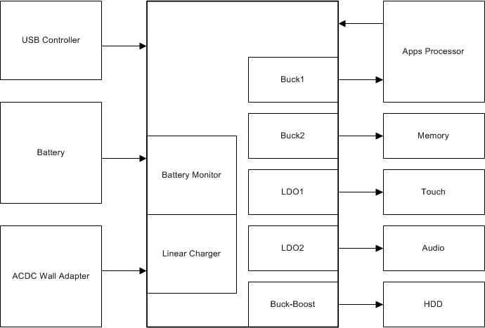
The LP3910 is a programmable system power management unit optimized for HDD-based portable media players. The device incorporates two low-dropout LDO voltage regulators, two integrated buck DC-DC converters with dynamic voltage scaling (DVS), one wide load-range buck-boost DC-DC converter with programmable output voltage, a 4-channel, 8-bit ADC, and a dual-source lithium-ion or lithium-polymer battery charger.
The LP3910 also incorporates some advanced battery management functions such as battery temperature measurement, reverse current blocking for USB, LED-charger status indication, thermally regulated internal power FETs, battery-voltage monitoring, overcurrent protection, and a 10-hour safety timer. The device is programmable through a 400-kHz I2C-compatible interface.
The LP3910 is available in a thermally-enhanced
6-mm × 6-mm × 0.8-mm 48-pin WQFN package.
Device Information(1)
| PART NUMBER | PACKAGE | BODY SIZE (NOM) |
|---|---|---|
| LP3910 | WQFN (48) | 6.00 mm × 6.00 mm |
Simplified Block Diagram
