SCLS261O October 1995 – September 2015 SN54AHC541 , SN74AHC541
- 1 Features
- 2 Applications
- 3 Description
- 4 Revision History
- 5 Pin Configuration and Functions
-
6 Specifications
- 6.1 Absolute Maximum Ratings
- 6.2 ESD Ratings
- 6.3 Recommended Operating Conditions
- 6.4 Thermal Information
- 6.5 Electrical Characteristics
- 6.6 Switching Characteristics, VCC = 3.3 V ± 0.3 V
- 6.7 Switching Characteristics, VCC = 5 V ± 0.5 V
- 6.8 Noise Characteristics
- 6.9 Operating Characteristics
- 6.10 Typical Characteristics
- 7 Parameter Measurement Information
- 8 Detailed Description
- 9 Application and Implementation
- 10Power Supply Recommendations
- 11Layout
- 12Device and Documentation Support
- 13Mechanical, Packaging, and Orderable Information
Package Options
Refer to the PDF data sheet for device specific package drawings
Mechanical Data (Package|Pins)
- W|20
- J|20
- FK|20
Thermal pad, mechanical data (Package|Pins)
Orderable Information
1 Features
2 Applications
- Servers
- PCs and Notebooks
- Network Switches
- Wearable Health and Fitness Devices
- Telecom Infrastructures
- Electronic Points-of-Sale
3 Description
The SNx4AHC541 octal buffers and drivers are ideal for driving bus lines or buffer memory address registers. These devices feature inputs and outputs on opposite sides of the package to facilitate printed circuit board layout.
Device Information(1)
| PART NUMBER | PACKAGE | BODY SIZE (NOM) |
|---|---|---|
| SNx4AHC541N | PDIP (20) | 25.40 mm x 6.35 mm |
| SNx4AHC541DB | SSOP (20) | 7.50 mm x 5.30 mm |
| SNx4AHC541PW | TSSOP (20) | 6.50 mm x 4.40 mm |
| SNx4AHC541DGV | TVSOP (20) | 5.00 mm x 4.40 mm |
| SNx4AHC541DW | SOIC (20) | 12.80 mm x 7.50 mm |
- For all available packages, see the orderable addendum at the end of the data sheet.
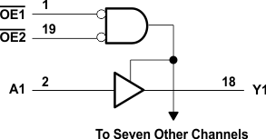
Simplified Block Diagram
