SLOS547A November 2008 – November 2015 THS4509-Q1
PRODUCTION DATA.
- 1 Features
- 2 Applications
- 3 Description
- 4 Revision History
- 5 Pin Configuration and Functions
- 6 Specifications
- 7 Detailed Description
-
8 Application and Implementation
- 8.1 Application Information
- 8.2 Typical Applications
- 9 Power Supply Recommendations
- 10Layout
- 11Device and Documentation Support
- 12Mechanical, Packaging, and Orderable Information
Package Options
Mechanical Data (Package|Pins)
- RGT|16
Thermal pad, mechanical data (Package|Pins)
- RGT|16
Orderable Information
1 Features
- Qualified for Automotive Applications
- Fully Differential Architecture
- Centered Input Common-Mode Range
- Minimum Gain of 2 V/V (6 dB)
- Bandwidth: 1900 MHz
- Slew Rate: 6600 V/μs
- 1% Settling Time: 2 ns
- HD2: –75 dBc at 100 MHz
- HD3: –80 dBc at 100 MHz
- OIP2: 73 dBm at 70 MHz
- OIP3: 37 dBm at 70 MHz
- Input Voltage Noise: 1.9 nV/√Hz (f > 10 MHz)
- Noise Figure: 17.1 dB
- Output Common-Mode Control
- Power Supply:
- Voltage: 3 V (±1.5 V) to 5 V (±2.5 V)
- Current: 37.7 mA
- Power-Down Capability: 0.65 mA
2 Applications
- Adaptive Cruise Control
- Blind Spot Detection
- Collision Warning
- Industrial
- 5-V Data Acquisition Systems High Linearity ADC Amplifier
- Test and Measurement
3 Description
The THS4509-Q1 is a wideband, fully differential operational amplifier designed for 5-V data-acquisition systems. It has very low noise at 1.9 nV/√Hz, and extremely low harmonic distortion of –75-dBc HD2 and –80-dBc HD3 at 100 MHz with 2 Vpp, G = 10 dB, and 1-kΩ load. Slew rate is very high at 6600 V/μs and with settling time of 2 ns to 1% (2-V step), it is ideal for pulsed applications. It is designed for minimum gain of 6 dB but is optimized for gain of 10 dB.
To allow for dc coupling to analog-to-digital converters (ADCs), its unique output common-mode control circuit maintains the output common-mode voltage within 3-mV offset (typical) from the set voltage, when set within 0.5 V of mid-supply, with less than 4-mV differential offset voltage. The common-mode set point is set to mid-supply by internal circuitry, which may be overdriven from an external source.
The input and output are optimized for best performance with their common-mode voltages set to mid-supply. Along with high-performance at low power-supply voltage, this makes for extremely high-performance single-supply 5-V data-acquisition systems.
The THS4509-Q1 is offered in a quad 16-pin leadless QFN package (RGT) and is characterized for operation over the full automotive temperature range from –40°C to 125°C.
Device Information(1)
| PART NUMBER | MINIMUM GAIN | COMMON-MODE RANGE OF INPUT |
|---|---|---|
| THS4509-Q1 | 6 dB | 0.75 V to 4.25 V |
- For all available packages, see the orderable addendum at the end of the data sheet.
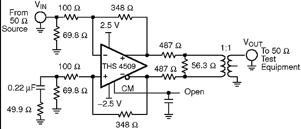
Simplified Schematic
