SLIS177 May 2016 TLC6C598
PRODUCTION DATA.
- 1 Features
- 2 Applications
- 3 Description
- 4 Revision History
- 5 Pin Configuration and Functions
- 6 Specifications
- 7 Parameter Measurement Information
- 8 Detailed Description
- 9 Application and Implementation
- 10Power Supply Recommendations
- 11Layout
- 12Device and Documentation Support
- 13Mechanical, Packaging, and Orderable Information
Package Options
Mechanical Data (Package|Pins)
- PW|16
Thermal pad, mechanical data (Package|Pins)
Orderable Information
1 Features
- Wide VCC From 3 V to 5.5 V
- Output Maximum Rating of 40 V
- Eight Power DMOS Transistor Outputs of 50-mA Continuous Current With VCC = 5 V or 200-mA PWM Current With Single-Pulse Duration Less Than 1 ms and Average Current Less Than 50 mA
- Thermal Shutdown Protection
- Enhanced Cascading for Multiple Stages
- All Registers Cleared With Single Input
- Low Power Consumption
- Slow Switching Time (tr and tf), Which Helps Significantly With Reducing EMI
- 16-Pin TSSOP-PW Package
2 Applications
- Appliance Display Panel
- Elevator Display Panel
- PLC Function Indicator
- Seven-Segment Display
3 Description
The TLC6C598 device is a monolithic, medium-voltage, low-current power 8-bit shift register designed for use in systems that require relatively moderate load power, such as LEDs.
This device contains an 8-bit serial-in, parallel-out shift register that feeds an 8-bit D-type storage register. Separate clocks are provided for both the shift and storage register. Outputs are low-side, open-drain DMOS transistors with output ratings of 40 V and 50 mA continuous sink-current OR 200-mA PWM current with single-pulse duration less than 1 ms and average current less than 50 mA capabilities when VCC = 5 V. The device contains built-in thermal shutdown protection and provides up to 2000 V of ESD protection when tested using the human-body model and the 200 V machine model.
The TLC6C598 characterization is for operation over the operating ambient temperature range of −40°C to 105°C.
Device Information(1)
| PART NUMBER | PACKAGE | BODY SIZE (NOM) |
|---|---|---|
| TLC6C598 | TSSOP (16) | 5.00 mm x 4.40 mm |
- For all available packages, see the orderable addendum at the end of the datasheet.
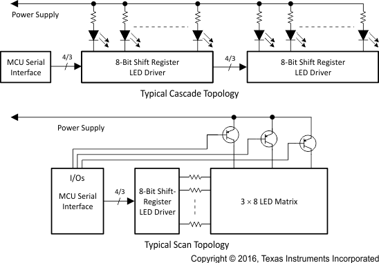
Typical Application Schematic
