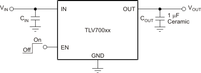
SLVSB67C November 2011 – June 2017 TLV70012-Q1 , TLV70018-Q1
PRODUCTION DATA.
- 1 Features
- 2 Applications
- 3 Description
- 4 Revision History
- 5 Pin Configuration and Functions
- 6 Specifications
- 7 Detailed Description
- 8 Application and Implementation
- 9 Power Supply Recommendations
- 10Layout
- 11Device and Documentation Support
- 12Mechanical, Packaging, and Orderable Information
Package Options
Mechanical Data (Package|Pins)
- DDC|5
Thermal pad, mechanical data (Package|Pins)
Orderable Information
1 Features
- Qualified for Automotive Applications
- AEC-Q100 Qualified With the Following Results:
- Device Temperature Grade 1: –40°C to 125°C Ambient Operating Temperature Range
- Device HBM ESD Classification Level H2
- Device CDM ESD Classification Level C3B
- 2% Accuracy
- Low IQ: 35 μA
- Fixed-Output Voltages: 1.2 V and 1.8 V
- High PSRR: 68 dB at 1 kHz
- Stable With Effective Capacitance of 0.1 μF(1)
- Thermal Shutdown and Overcurrent Protection (1)
2 Applications
- Automotive Head Units
- Camera Sensors and Modules
- Heads-Up Displays (HUD)
- Telematics Control Units
3 Description
The TLV70018-Q1 and TLV70012-Q1 low-dropout (LDO) linear regulators are low quiescent current devices with excellent line and load transient performance. A precision band-gap and error amplifier provides overall 2% accuracy. Low output noise, high power-supply rejection ratio (PSRR), and low-dropout voltage make this series of devices ideal for powering power-sensitive loads. All device versions have thermal shutdown and current limit for detecting fault conditions.
Furthermore, these devices are stable with an effective output capacitance of only 0.1 μF. This feature enables the use of cost-effective capacitors that have higher bias voltages and temperature derating. The devices regulate to specified accuracy with no output load.
Device Information(1)
| PART NUMBER | PACKAGE | BODY SIZE (NOM) |
|---|---|---|
| TLV70018-Q1 | SOT (5) | 2.90 mm × 1.60 mm |
| TLV70012-Q1 |
- For all available packages, see the orderable addendum at the end of the data sheet.
SPACE
SPACE
SPACE
SPACE
SPACE
SPACE
