SLIS093D March 2000 – March 2015 TPIC6C596
PRODUCTION DATA.
- 1 Features
- 2 Applications
- 3 Description
- 4 Revision History
- 5 Pin Configuration and Functions
- 6 Specifications
- 7 Parameter Measurement Information
- 8 Detailed Description
- 9 Application and Implementation
- 10Power Supply Recommendations
- 11Layout
- 12Device and Documentation Support
- 13Mechanical, Packaging, and Orderable Information
Package Options
Refer to the PDF data sheet for device specific package drawings
Mechanical Data (Package|Pins)
- PW|16
- N|16
- D|16
Thermal pad, mechanical data (Package|Pins)
- D|16
Orderable Information
1 Features
2 Applications
- Instrumentation Clusters
- Tell-Tale Lamps
- LED Illumination and Controls
- Automotive Relay or Solenoids Drivers
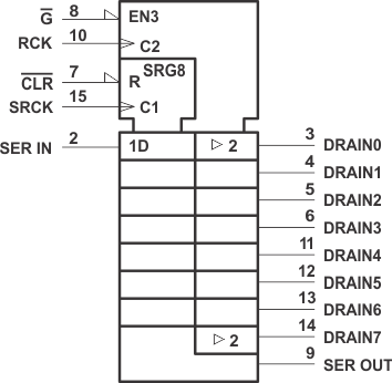
Logic Symbol

3 Description
The TPIC6C596 device is a monolithic, medium-voltage, low-current, 8-bit shift register designed for use in systems that require relatively moderate load power such as LEDs. The device contains a built-in voltage clamp on the outputs for inductive transient protection. Power driver applications include relays, solenoids, and other low-current or medium-voltage loads.
This device contains an 8-bit serial-in, parallel-out shift register that feeds an 8-bit D-type storage register. Data transfers through both the shift and storage registers on the rising edge of the shift register clock (SRCK) and the register clock (RCK), respectively. The storage register transfers data to the output buffer when shift register clear (CLR) is high. When CLR is low, all registers in the device are cleared. When output enable (G) is held high, all data in the output buffers is held low and all drain outputs are off. When G is held low, data from the storage register is transparent to the output buffers. When data in the output buffers is low, the DMOS transistor outputs are off. When data is high, the DMOS transistor outputs have sink-current capability.
The serial output (SER OUT) is clocked out of the device on the falling edge of SRCK to provide additional hold time for cascaded applications. This will provide improved performance for applications where clock signals may be skewed, devices are not located near one another, or the system must tolerate electromagnetic interference.
Outputs are low-side, open-drain DMOS transistors with output ratings of 33 V and 100 mA continuous sink-current capability. Each output provides a 250-mA maximum current limit at TC = 25°C. The current limit decreases as the junction temperature increases for additional device protection. The device also provides up to 2500 V of ESD protection when tested using the human body model and the 200-V machine model.
The TPIC6C596 device is characterized for operation over the operating case temperature range of −40°C to 125°C.
Device Information(1)
| PART NUMBER | PACKAGE | BODY SIZE (NOM) |
|---|---|---|
| TPIC6C596 | SOIC (16) | 9.90 mm × 3.91 mm |
| PDIP (16) | 19.30 mm × 6.35 mm | |
| TSSOP (16) | 5.00 mm × 4.40 mm |
- For all available packages, see the orderable addendum at the end of the data sheet.
4 Revision History
Changes from C Revision (April 2005) to D Revision
- Added ESD Ratings table, Feature Description section, Device Functional Modes, Application and Implementation section, Power Supply Recommendations section, Layout section, Device and Documentation Support section, and Mechanical, Packaging, and Orderable Information section Go