SLVSCH2 July 2014 TPS2105-EP
PRODUCTION DATA.
- 1 Features
- 2 Applications
- 3 Description
- 4 Revision History
- 5 Pin Configuration and Functions
- 6 Specifications
- 7 Detailed Description
- 8 Application and Implementation
- 9 Power Supply Recommendations
- 10Layout
- 11Device and Documentation Support
- 12Mechanical, Packaging, and Orderable Information
Package Options
Mechanical Data (Package|Pins)
- DBV|5
Thermal pad, mechanical data (Package|Pins)
Orderable Information
1 Features
- Dual-Input, Single-Output MOSFET Switch With No Reverse Current Flow (No Parasitic Diodes)
- IN1: 250-mΩ, 500-mA N-Channel; 18-µA Supply Current
- IN2: 1.3-mΩ, 100-mA P-Channel; 0.75-µA Supply Current (VAUX Mode)
- Advanced Switch Control Logic
- CMOS and TTL Compatible Enable Input
- Controlled Rise, Fall, and Transition Times
- 2.7-V to 5.5-V Operating Range
- SOT-23-5 Package
- 2-kV Human Body Model, 750-V Charged Device Model, 200-V Machine-Model ESD Protection
- Supports Defense, Aerospace, and Medical Applications
- Controlled Baseline
- One Assembly and Test Site
- One Fabrication Site
- Available in Military (–55°C to 125°C) Temperature Range
- Extended Product Life Cycle
- Extended Product-Change Notification
- Product Traceability
2 Applications
- Notebook and Desktop PCs
- Cell phone, Palmtops, and PDAs
- Battery Management
3 Description
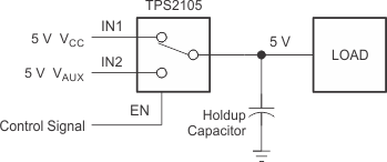
The TPS2105 is a dual-input, single-output power switch designed to provide uninterrupted output voltage when transitioning between two independent power supplies. Both devices combine one N-channel (250 mΩ) and one P-channel (1.3-Ω) MOSFET with a single output. The P-channel MOSFET (IN2) is used with auxiliary power supplies that deliver lower current for standby modes. The N-channel MOSFET (IN1) is used with a main power supply that delivers higher current required for normal operation. Low on-resistance makes the N-channel the ideal path for higher main supply current when power-supply regulation and system voltage drops are critical. When using the P-channel MOSFET, quiescent current is reduced to 0.75 µA to decrease the demand on the standby power supply. The MOSFETs in the TPS2105 do not have the parasitic diodes, typically found in discrete MOSFETs, thereby preventing back-flow current when the switch is off.
Device Information(1)
| ORDER NUMBER | PACKAGE | BODY SIZE (NOM) |
|---|---|---|
| TPS2105MDBVREP | SOT-23 (5) | 2.90 mm × 1.60 mm |
- For all available packages, see the orderable addendum at the end of the data sheet.
Simplified Schematic