SLUSCX9 March 2017 TPS53627
PRODUCTION DATA.
- 1Features
- 2Applications
- 3Description
- 4Revision History
- 5Device and Documentation Support
- 6Mechanical, Packaging, and Orderable Information
Package Options
Mechanical Data (Package|Pins)
- RSM|32
Thermal pad, mechanical data (Package|Pins)
- RSM|32
Orderable Information
1 Features
- Intel® VR13 Serial VID (SVID) Compliant
- 1- or 2-Phase Operation
- Supports Both Droop and Non-Droop Applications
- 8-Bit DAC with 10-mV Step
- 4.5-V to 28-V Conversion Voltage Range
- Output Range: 0.5 V to 2.3 V
- Optimized Efficiency at Light and Heavy Loads
- 8 Independent Levels of Overshoot Reduction (OSR) and Undershoot Reduction (USR)
- Driverless Configuration for Efficient High-Frequency Switching
- Supports Discrete, Power Block, Power Stage™ or DrMOS MOSFET Implementations
- Accurate, Adjustable Voltage Positioning
- 300-kHz to 1-MHz Frequency Selections
- Patented AutoBalance™ Phase Balancing
- Programmable ON-Pulse Extension for Load Transient Boost
- Programmable Auto DCM and CCM Operation
- Selectable 8-level Current Limit
- Small, 4 mm × 4 mm, 32-Pin, VQFN PowerPad™ Package
2 Applications
- VDDQ for DDR Memory
- SoC Processor VCORE Power
3 Description
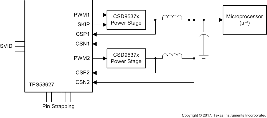
The TPS53627 device is a driverless, VR13 SVID compliant, synchronous buck controller. Advanced control features such as D-CAP+ ™architecture with overlapping pulse support undershoot reduction (USR) and overshoot reduction (OSR) to provide fast transient response, lowest output capacitance and high efficiency. The device also supports single-phase operation in CCM and DCM operation for light-load efficiency boost. The device integrates a full set of VR13 I/O features including VR_READY (PGOOD), ALERT and VR_HOT. The SVID interface address allows programming from 00h to 07h. Adjustable control of VOUT slew rate can be programmed as high as 20mV/uS.
Paired with the TI NexFET™ Power Stage, this total solution delivers exceptionally high speed and low switching loss.
The TPS53627 device package is a space saving, thermally enhanced 32-pin VQFN package that operates from –40°C to +105°C.
Device Information(1)
| PART NUMBER | PACKAGE | BODY SIZE (NOM) |
|---|---|---|
| TPS53627 | VQFN (32) | 4.00 mm × 4.00 mm |
- For all available packages, see the orderable addendum at the end of the document.
.. Simplified Schematic
