SLVSA18A September 2009 – July 2015 TPS61161-Q1
PRODUCTION DATA.
- 1 Features
- 2 Applications
- 3 Description
- 4 Revision History
- 5 Pin Configuration and Functions
- 6 Specifications
- 7 Detailed Description
- 8 Applications and Implementation
- 9 Power Supply Recommendations
- 10Layout
- 11Device and Documentation Support
- 12Mechanical, Packaging, and Orderable Information
Package Options
Mechanical Data (Package|Pins)
- DRV|6
Thermal pad, mechanical data (Package|Pins)
- DRV|6
Orderable Information
1 Features
2 Applications
- Automotive Cluster Backlighting
- High-Brightness LED Lighting
- White LED Backlighting Media Form Factor Displays
3 Description
With a 40-V rated integrated switch FET, the TPS61161-Q1 is a boost converter that drives up to 10 LEDs in series. The boost converter runs at 600-kHz fixed switching frequency to reduce output ripple, improve conversion efficiency, and allow for the use of small external components.
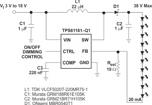
The default white LED current is set with the external sensor resistor Rset, and the feedback voltage is regulated to 200 mV, as shown in the typical application. During the operation, the LED current can be controlled using the 1-wire digital interface (EasyScale™ protocol) through the CTRL pin. Alternatively, a pulse width modulation (PWM) signal can be applied to the CTRL pin through which the duty cycle determines the feedback reference voltage. In either digital or PWM mode, the TPS61161-Q1 does not burst the LED current; therefore, it does not generate audible noises on the output capacitor. For maximum protection, the device features integrated open LED protection that disables the TPS61161-Q1 to prevent the output from exceeding the absolute maximum ratings during open LED conditions.
The TPS61161 is available in a space-saving, 2-mm × 2-mm QFN (DRV) package with thermal pad.
Device Information(1)
| PART NUMBER | PACKAGE | BODY SIZE (NOM) |
|---|---|---|
| TPS61161-Q1 | SON (6) | 2.00 mm × 2.00 mm |
- For all available packages, see the orderable addendum at the end of the data sheet.
Typical Application
