SLVS149C June 2003 – September 2015 TPS65010
PRODUCTION DATA.
- 1 Features
- 2 Applications
- 3 Description
- 4 Revision History
- 5 Pin Configuration and Functions
- 6 Specifications
-
7 Detailed Description
- 7.1 Overview
- 7.2 Functional Block Diagram
- 7.3
Feature Description
- 7.3.1
Battery Charger
- 7.3.1.1 Autonomous Power Source Selection
- 7.3.1.2 Temperature Qualification
- 7.3.1.3 Battery Preconditioning
- 7.3.1.4 Battery Charge Current
- 7.3.1.5 Battery Voltage Regulation
- 7.3.1.6 Charge Termination and Recharge
- 7.3.1.7 Sleep Mode
- 7.3.1.8 PG Output
- 7.3.1.9 Thermal Considerations for Setting Charge Current
- 7.3.2 Step-Down Converters, VMAIN and VCORE
- 7.3.3 Low-Dropout Voltage Regulators
- 7.3.4 Undervoltage Lockout
- 7.3.5 Power-Up Sequencing
- 7.3.6 System Reset and Control Signals
- 7.3.7 Vibrator Driver
- 7.3.1
Battery Charger
- 7.4 Device Functional Modes
- 7.5 Programming
- 7.6
Register Maps
- 7.6.1 CHGSTATUS Register (Address: 01h—Reset: 00h)
- 7.6.2 REGSTATUS Register (Address: 02h—Reset: 00h)
- 7.6.3 MASK1 Register (Address: 03h—Reset: FFh)
- 7.6.4 MASK2 Register (Address: 04h—Reset: FFh)
- 7.6.5 ACKINT1 Register (Address: 05h—Reset: 00h)
- 7.6.6 ACKINT2 Register (Address: 06h—Reset: 00h)
- 7.6.7 CHGCONFIG Register Address: 07h—Reset: 1Bh
- 7.6.8 LED1_ON Register (Address: 08h—Reset: 00h)
- 7.6.9 LED1_PER Register (Address: 09h—Reset: 00h)
- 7.6.10 LED2_ON Register (Address: 0Ah—Reset: 00h)
- 7.6.11 LED2_PER (Register Address: 0Bh—Reset: 00h)
- 7.6.12 VDCDC1 Register (Address: 0Ch—Reset: 72h/73h)
- 7.6.13 VDCDC2 Register (Address: 0Dh—Reset: 68h/78h)
- 7.6.14 VREGS1Register (Address: 0Eh—Reset: 88h)
- 7.6.15 MASK3 Register (Address: 0Fh—Reset: 00h)
- 7.6.16 DEFGPIO Register Address: (10h—Reset: 00h)
- 8 Application and Implementation
- 9 Power Supply Recommendations
- 10Layout
- 11Device and Documentation Support
- 12Mechanical, Packaging, and Orderable Information
Package Options
Mechanical Data (Package|Pins)
- RGZ|48
Thermal pad, mechanical data (Package|Pins)
- RGZ|48
Orderable Information
1 Features
- Linear Charger Management for Single Li-Ion or Li-Polymer Cells
- Dual Input Ports for Charging From USB or From Wall Plug, Handles 100-mA and 500-mA USB Requirements
- Charge Current Programmable Through External Resistor
- 1-A, 95% Efficient Step-Down Converter for I/O and Peripheral Components (VMAIN)
- 400-mA, 90% Efficient Step-Down Converter for Processor Core (VCORE)
- 2x 200-mA LDOs for I/O and Peripheral Components, LDO Enable Through Bus
- Serial Interface Compatible With I2C, Supports 100-kHz, 400-kHz Operation
- LOW_PWR Pin to Lower or Disable Processor Core Supply Voltage in Deep Sleep Mode
- 70-µA Quiescent Current
- 1% Reference Voltage
- Thermal Shutdown Protection
2 Applications
- All Single Li-Ion Cell Operated Products Requiring Multiple Supplies Including:
- PDA
- Cellular and Smart Phone
- Internet Audio Player
- Digital Still Camera
- Digital Radio Player
- Split Supply DSP and µP Solutions
3 Description
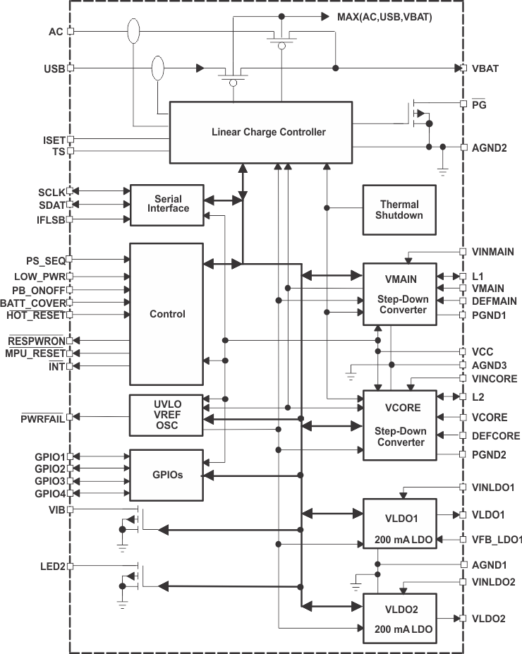
The TPS65010 device is an integrated power and battery management IC for applications powered by one Li-Ion or Li-Polymer cell, and which require multiple power rails. The TPS65010 provides two highly efficient, 1.25-MHz step-down converters targeted at providing the core voltage and peripheral, I/O rails in a processor-based system. Both step-down converters enter a low-power mode at light load for maximum efficiency across the widest possible range of load currents. The TPS65010 also integrates two 200-mA LDO voltage regulators, which are enabled through the serial interface. Each LDO operates with an input voltage range from 1.8 V to 6.5 V, thus allowing them to be supplied from one of the step-down converters or directly from the battery.
The TPS65010 also has a highly integrated and flexible Li-Ion linear charger and system power management. It offers integrated USB-port and AC-adapter supply management with autonomous power-source selection, power FET and current sensor, high accuracy current and voltage regulation, charge status, and charge termination.
Device Information(1)
| PART NUMBER | PACKAGE | BODY SIZE (NOM) |
|---|---|---|
| TPS65010 | VQFN (48) | 7.00 mm x 7.00 mm |
- For all available packages, see the orderable addendum at the end of the datasheet.
Block Diagram

4 Revision History
Changes from B Revision (January 2005) to C Revision
- Added Pin Configuration and Functions section, ESD Ratings table, Feature Description section, Device Functional Modes, Application and Implementation section, Power Supply Recommendations section, Layout section, Device and Documentation Support section, and Mechanical, Packaging, and Orderable Information section Go