SLVSBX4C June 2013 – May 2017 TPS65150-Q1
PRODUCTION DATA.
- 1 Features
- 2 Applications
- 3 Description
- 4 Revision History
- 5 Pin Configuration and Functions
- 6 Specifications
- 7 Detailed Description
-
8 Application and Implementation
- 8.1 Application Information
- 8.2
Typical Application
- 8.2.1 Design Requirements
- 8.2.2
Detailed Design Procedure
- 8.2.2.1 Boost Converter Design Procedure
- 8.2.2.2 Rectifier Diode Selection
- 8.2.2.3 Setting the Output Voltage
- 8.2.2.4 Output Capacitor Selection
- 8.2.2.5 Input Capacitor Selection
- 8.2.2.6 Compensation
- 8.2.2.7 Negative Charge Pump
- 8.2.2.8 Positive Charge Pump
- 8.2.2.9 Gate Voltage Shaping
- 8.2.2.10 Power-On Sequencing
- 8.2.2.11 Fault Delay
- 8.2.3 Application Curves
- 8.3 System Examples
- 9 Power Supply Recommendations
- 10Layout
- 11Device and Documentation Support
- 12Mechanical, Packaging, and Orderable Information
Package Options
Mechanical Data (Package|Pins)
- PWP|24
Thermal pad, mechanical data (Package|Pins)
- PWP|24
Orderable Information
1 Features
- AEC-Q100 Qualified:
- Device Temperature Grade 1: –40°C to 125°C Junction Temperature
- Device HBM ESD Classification According to AEC - Q100-002
- Device CDM ESD Classification According to AEC - Q100-011
- Input Voltage Range: 1.8 V to 6 V
- V(VS) Boost Converter
- Up to 15 V Output Voltage
- < 1% Output Voltage Accuracy
- 2-A Switch Current Limit
- V(VGH) Positive Regulated Charge Pump Driver
- Up to 30 V Output Voltage
- Gate Voltage Shaping
- V(VGL) Negative Regulated Charge Pump Driver
- Down to –15 V Output Voltage
- Integrated VCOM Buffer
- Adjustable Power On Sequencing
- Gate Drive Signal for External Isolation MOSFET for V(VS)
- Protection Features
- Out-of-Regulation Protection
- Over-voltage Protection
- Adjustable Fault Detection Timing
- Thermal Shutdown
- 24-Pin TSSOP Package with Exposed Thermal Pad
2 Applications
- LCD Displays ranging approx. from 4" to 17"
- Automotive Infotainment & Cluster
- Automotive Navigation Systems
- Rear Seat Entertainment
- Smart Mirror
3 Description
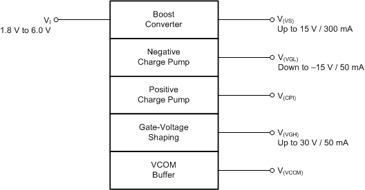
The TPS65150-Q1 is an integrated power-supply for automotive LCD applications. The device integrates a boost converter for the source voltage and two regulated adjustable charge pump drivers for the gate voltages. For reduced external cost, improved picture quality and reduced image sticking, the device includes a VCOM buffer and a gate-voltage shaping function.
The device is designed to operate from a supply voltage of 1.8 V to 6 V making it ideal for automotive LCD applications using a fixed 3.3 V or 5 V input-voltage rail.
Adjustable power-on sequencing for VGL and VGH allow the device to be optimized for a variety of displays.
For protection from system malfunction, the TPS65150-Q1 integrates an adjustable shutdown latch feature. The device monitors the outputs (V(VS), V(VGL), V(VGH)); and, as soon as one of the outputs falls below its power-good threshold for longer than the adjustable fault delay time, the device enters shutdown.
Device Information(1)
| PART NUMBER | PACKAGE | BODY SIZE (NOM) |
|---|---|---|
| TPS65150-Q1 | TSSOP (24) | 6.40 mm × 7.80 mm |
- For all available packages, see the orderable addendum at the end of the data sheet.
Block Diagram
