SLVSCT9B November 2014 – January 2015 TPS65266
PRODUCTION DATA.
- 1 Features
- 2 Applications
- 3 Description
- 4 Revision History
- 5 Pin Configuration and Functions
- 6 Specifications
-
7 Detailed Description
- 7.1 Overview
- 7.2 Functional Block Diagram
- 7.3
Feature Description
- 7.3.1 Adjusting the Output Voltage
- 7.3.2 Enable and Adjusting UVLO
- 7.3.3 Soft-Start Time
- 7.3.4 Power-Up Sequencing
- 7.3.5 Boostrap Voltage and BST-LX UVLO
- 7.3.6 Out of Phase Operation
- 7.3.7 Output Overvoltage Protection (OVP)
- 7.3.8 Slope Compensation
- 7.3.9 Overcurrent Protection
- 7.3.10 Power Good
- 7.3.11 Adjustable Switching Frequency
- 7.3.12 Thermal Shutdown
- 7.4 Device Functional Modes
- 8 Application and Implementation
- 9 Power Supply Recommendations
- 10Layout
- 11Device and Documentation Support
- 12Mechanical, Packaging, and Orderable Information
Package Options
Mechanical Data (Package|Pins)
- RHB|32
Thermal pad, mechanical data (Package|Pins)
- RHB|32
Orderable Information
1 Features
- Operating Input Voltage Range 2.7 to 6.5 V
- Feedback Reference Voltage 0.6 V ±1%
- Maximum Continuous Output Current 3 A/2 A/2 A
- Dedicated Enable and Soft Start
- Accurate Start-Up Timing Control With Enable Pins Discharge
- Forced Continuous Current (FCC) Mode at Light Load
- Cycle-by-Cycle Current Limiting With Hiccup Mode Overcurrent Protection
- Adjustable Clock Frequency 250 kHz to 2.4 MHz
- External Clock Synchronization
- Power-Good Indicator
- Overtemperature Protection
2 Applications
- Printer and Scanner
- Digital TV
- Set Top Box
- Home Gateway and Access Point Networks
- Surveillance
3 Description
The TPS65266 incorporates 3 channels of high-efficiency synchronous buck converter for applications operating off the adaptor or battery with input voltage lower than 6.5 V.
The buck DC/DC converter integrates power MOSFETs for optimized power efficiency and reduces external component counts. The peak current mode control simplifies the compensation and fast transient response. High clock frequency allows smaller and low-value inductors and capacitors. External compensation supports optimized loop compensation and fast transient response. In light load condition, the buck converter operates in FCC mode for a reduction in noise susceptibility and RF interference. Cycle-by-cycle overcurrent limiting with hiccup mode limits MOSFET power dissipation in short circuit or overloading fault conditions.
The TPS65266 features a power-good supervisor circuit that monitors all converter outputs. The PGOOD pin is asserted after the output voltages in each channel are in regulation and sequencing is done.
When continuous heavy overload or short circuit increases power dissipation in the buck converter, internal thermal protection circuit shuts off the device to prevent damage. Recovery from a thermal shutdown is automatic after the device has cooled sufficiently.
Device Information(1)
| PART NUMBER | PACKAGE | BODY SIZE (NOM) |
|---|---|---|
| TPS65266 | VQFN (32) | 5.00 mm × 5.00 mm |
- For all available packages, see the orderable addendum at the end of the data sheet.
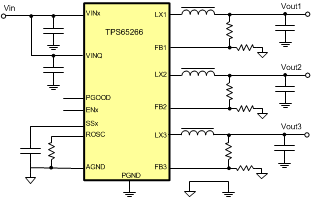
Simplified Application Schematic
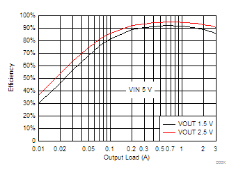
Efficiency vs Output Load