SLVSAS4J June 2013 – April 2017 TPS7H1201-HT
PRODUCTION DATA.
- 1 Features
- 2 Applications
- 3 Description
- 4 Revision History
- 5 Pin Configuration and Functions
- 6 Specifications
- 7 Detailed Description
- 8 Application and Implementation
- 9 Power Supply Recommendations
- 10Layout
- 11Device and Documentation Support
- 12Mechanical, Packaging, and Orderable Information
Package Options
Mechanical Data (Package|Pins)
- HKS|16
- KGD|0
Thermal pad, mechanical data (Package|Pins)
Orderable Information
1 Features
- Wide VIN Range: 1.5 V to 7 V
- Current Share/Parallel Operation to Provide Higher Output Current
- Stable With Ceramic Output Capacitor
- ±4.2% Accuracy Over Line, Load, and Temperature
- Programmable Soft-Start
- Power-Good Output
- LDO Voltage:
100 mV (Max) at 0.5 A (210°C), VOUT = 6.8 V - Low Noise:
20.26 µVRMS VIN = 2.1 V, VOUT = 1.8 V at 0.5 A - PSRR: Over 45 dB at 1 kHz
- Load/Line Transient Response
- See the Tools & Software Tab
2 Applications
- RF 5-V Components VCOs, Receivers, ADCs, Amplifiers
- Clock Distribution
- Clean Analog Supply Requirements
- Supports Harsh Environment Applications
- Available in Extreme (–55°C to 210°C) Temperature Range(1)
- TI's High-Temperature Products Use Highly-Optimized Silicon (Die) Solutions With Design and Process Enhancements to Maximize Performance Over Extended Temperatures
3 Description
The TPS7H1201-HT is a LDO linear regulator that uses a PMOS pass element configuration. This device operates over a wide range of input voltage, from 1.5 V to 7 V while offering excellent PSRR.
The TPS7H1201-HT features a precise and programmable foldback current limit implementation with a very-wide adjustment range. To support the complex power requirements of FPGAs, DSPs, or microcontrollers, the TPS7H1201-HT provides enable on and off functionality, programmable SoftStart, current sharing capability, and a PowerGood open-drain output.
The TPS7H1201-HT is available in a thermally-enhanced 16-pin ceramic flatpack package (CFP) and KGD (bare die) package.
Device Information(2)
| PART NUMBER | PACKAGE | BODY SIZE (NOM) |
|---|---|---|
| TPS7H1201-HT | CFP (16) | 11.00 mm × 9.60 mm |
- Custom temperature ranges are available
- For all available packages, see the orderable addendum at the end of the data sheet.
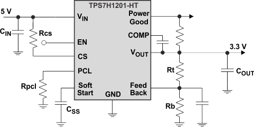
Typical Application Circuit
