SBAS484B September 2010 – December 2016 TSC2014
PRODUCTION DATA.
- 1 Features
- 2 Applications
- 3 Description
- 4 Revision History
- 5 Pin Configuration and Functions
-
6 Electrical Specifications
- 6.1 Absolute Maximum Ratings
- 6.2 ESD Ratings
- 6.3 Thermal Information
- 6.4 Recommended Operating Conditions
- 6.5 Electrical Characteristics
- 6.6 Timing Requirements for : I2C Standard Mode (fSCL = 100 kHz)
- 6.7 Timing Requirements for : I2C Fast Mode (fSCL = 400 kHz)
- 6.8 Timing Requirements for : I2C High-Speed Mode (fSCL = 1.7 MHz)
- 6.9 Timing Requirements for : I2C High-Speed Mode (fSCL = 3.4 MHz)
- 6.10 Timing Information
- 6.11 Typical Characteristics
-
7 Detailed Description
- 7.1 Overview
- 7.2 Functional Block Diagram
- 7.3 Feature Description
- 7.4 Device Functional Modes
- 7.5 Programming
- 7.6
Register Maps
- 7.6.1 R/W
- 7.6.2 Control Byte 0
- 7.6.3 Control Byte 1
- 7.6.4 Communication Protocol
- 7.6.5 Configuration Register 2
- 7.6.6 Converter Function Select Register
- 7.6.7 Data Registers
- 8 Application and Implementation
- 9 Power Supply Recommendations
- 10Layout
- 11Device and Documentation Support
- 12Mechanical, Packaging, and Orderable Information
Package Options
Mechanical Data (Package|Pins)
- YZG|12
Thermal pad, mechanical data (Package|Pins)
Orderable Information
1 Features
- 4-Wire Touch Screen Interface
- Ratiometric Conversion
- Single 1.2V to 3.6V Supply
- Preprocessing to Reduce Bus Activity
- High-Speed I2C-Compatible Interface
- Internal Detection of Screen Touch
- Register-Based Programmable:
- 10-Bit or 12-Bit Resolution
- Sampling Rates
- System Timing
- On-Chip Temperature Measurement
- Touch Pressure Measurement
- Auto Power-Down Control
- Low Power:
- 430μW at 1.8V, 50SSPS
- 320μW at 1.6V, 50SSPS
- 190μW at 1.2V, 50SSPS
- 58μW at 1.6V, 8.2kSPS Eq. Rate
- 37μW at 1.2V, 8.2kSPS Eq. Rate
- Enhanced ESD Protection:
- ±8kV HBM
- ±1kV CDM
- ±25kV Air Gap Discharge
- ±11kV Contact Discharge
- 1.5 x 2.0 WCSP-12 Package (1)
2 Applications
- Cellular Phones
- Portable Instruments
- MP3 Players, Pagers
- Multiscreen Touch Control
3 Description
The TSC2014 is a very low-power touch screen controller designed to work with power-sensitive, handheld applications that are based on advanced low-voltage processors. It works with a supply voltage as low as 1.2V, which can be supplied by a single-cell battery. It contains a complete, ultralow-power, 12-bit, analog-to-digital (A/D) resistive touch screen converter, including drivers and the control logic to measure touch pressure.
In addition to these standard features, the TSC2014 offers preprocessing of the touch screen measurements to reduce bus loading, thus reducing the consumption of host processor resources that can then be redirected to more critical functions.
The TSC2014 supports an I2C serial bus and data transmission protocol in all three defined modes: standard, fast, and high-speed. It offers programmable resolution of 10 or 12 bits to accommodate different screen sizes and performance needs.
The TSC2014 is available in a miniature, 12-lead,
3 x 4 array, (1.555 ±0.055)mm x (2.055 ±0.055)mm wafer chip-scale package (WCSP) package. The device is characterized for the –40°C to +85°C industrial temperature range.
Device Information(1)
| PART NUMBER | PACKAGE | BODY SIZE (NOM) |
|---|---|---|
| TSC2014 | DSBGA (12) | (1.555 ±0.055)mm x (2.055 ±0.055)mm |
- For all available packages, see the orderable addendum at the end of the data sheet.
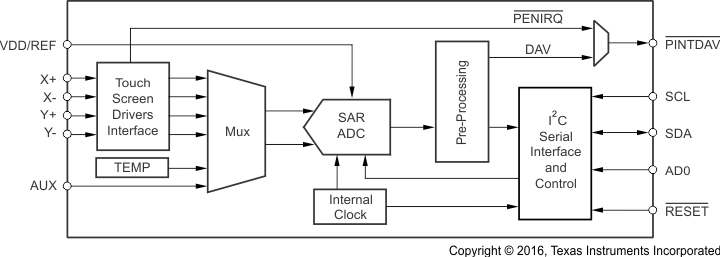
Block Diagram

4 Revision History
Changes from A Revision (February 2012) to B Revision
- Added Device Information table, ESD Ratings table, Recommended Operating Conditions table, Feature Description section, Device Functional Modes section, Application and Implementation sectionPower Supply Recommendations section, Layout section, Device and Documentation Support section, and Mechanical, Packaging, and Orderable Information sectionGo
- Deleted the ORDERING INFORMATION tableGo
Changes from * Revision (September 2010) to A Revision
- Changed notes for 100kHz Timing Requirements tableGo
- Changed notes for 400kHz Timing Requirements tableGo
- Changed notes for 1.7MHz Timing Requirements tableGo
- Changed Fall Time for SDA Signal from 20ns to 1ns for 1.7MHz Timing Requirements tableGo
- Changed notes for 3.4MHz Timing Requirements tableGo
- Changed Fall Time for SDA Signal from 10ns to 1ns for 3.4MHz Timing Requirements tableGo