SNAS298G August 2005 – January 2015 ADC128S102
PRODUCTION DATA.
- 1 Features
- 2 Applications
- 3 Description
- 4 Revision History
- 5 Pin Configuration and Functions
- 6 Specifications
- 7 Detailed Description
- 8 Application and Implementation
- 9 Power Supply Recommendations
- 10Layout
- 11Device and Documentation Support
- 12Mechanical, Packaging, and Orderable Information
Package Options
Mechanical Data (Package|Pins)
- PW|16
Thermal pad, mechanical data (Package|Pins)
Orderable Information
8 Application and Implementation
NOTE
Information in the following applications sections is not part of the TI component specification, and TI does not warrant its accuracy or completeness. TI’s customers are responsible for determining suitability of components for their purposes. Customers should validate and test their design implementation to confirm system functionality.
8.1 Application Information
The ADC128S102 is a successive-approximation analog-to-digital converter designed around a charge- redistribution digital-to-analog converter. Since the ADC128S102 integrates an 8 to 1 MUX on the front end, the device is typically used in applications where multiple voltages need to be monitored. In addition to having 8 input channels, the ADC128S102 can operate at sampling rates up to 1 MSPS. As a result, the ADC128S102 is typically run in burst fashion where a voltage is sampled for several times and then the ADC128S102 can be powered-down. This is a common technique for applications that are power limited. Due to the high bandwidth and sampling rate, the ADC128S102 is suitable for monitoring AC waveforms as well as DC inputs. The following example shows a common configuration for monitoring AC inputs.
8.2 Typical Application
The following sections outline the design principles of data acquisition system based on the ADC128S102.
A typical application is shown in Figure 38. The analog supply is bypassed with a capacitor network located close to the ADC128S102. The ADC128S102 uses the analog supply (VA) as its reference voltage, so it is very important that VA be kept as clean as possible. Due to the low power requirements of the ADC128S102, it is also possible to use a precision reference as a power supply.
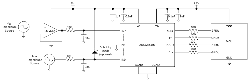 Figure 38. Typical Application Circuit
8.2.1 Design Requirements
A positive supply only data acquisition system capable of digitizing signals ranging 0 to 5 V, BW = 10 kHz, and a throughput of 125 kSPS.
The ADC128S102 has to interface to an MCU whose supply is set at 3.3 V.
8.2.2 Detailed Design Procedure
The signal range requirement forces the design to use 5-V analog supply at VA, analog supply. This follows from the fact that VA is also a reference potential for the ADC.
The requirement of interfacing to the MCU which is powered by 3.3-V supply, forces the choice of 3.3-V as a VD supply.
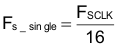
Sampling is in fact a modulation process which may result in aliasing of the input signal, if the input signal is not adequately band limited. The maximum sampling rate of the ADC128S102 when all channels are enabled is, Fs:

Note that faster sampling rates can be achieved when fewer channels are sampled. Single channel can be sampled at the maximum rate of:
In order to avoid the aliasing the Nyquist criterion has to be met:

Therefore it is necessary to place anti-aliasing filters at all inputs of the ADC. These filters may be single pole low pass filters whose pole location has to satisfy, assuming all channels sampled in sequence:
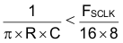
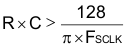
With Fsclk = 16 MHz, a good choice for the single pole filter is:
- R = 100
- C = 33 nF
This reduces the input BWsignal = 48 kHz. The capacitor at the INx input of the device provides not only the filtering of the input signal, but it also absorbs the charge kick-back from the ADC. The kick-back is the result of the internal switches opening at the end of the acquisition period.
The VA and VD sources are already separated in this example, due to the design requirements. This also benefits the overall performance of the ADC, as the potentially noisy VD supply does not contaminate the VA. In the same vain, further consideration could be given to the SPI interface, especially when the master MCU is capable of producing fast rising edges on the digital bus signals. Inserting small resistances in the digital signal path may help in reducing the ground bounce, and thus improve the overall noise performance of the system.
Care should be taken when the signal source is capable of producing voltages beyond VA. In such instances the internal ESD diodes may start conducting. The ESD diodes are not intended as input signal clamps. To provide the desired clamping action use Schottky diodes as shown in Figure 38.
8.2.3 Application Curve
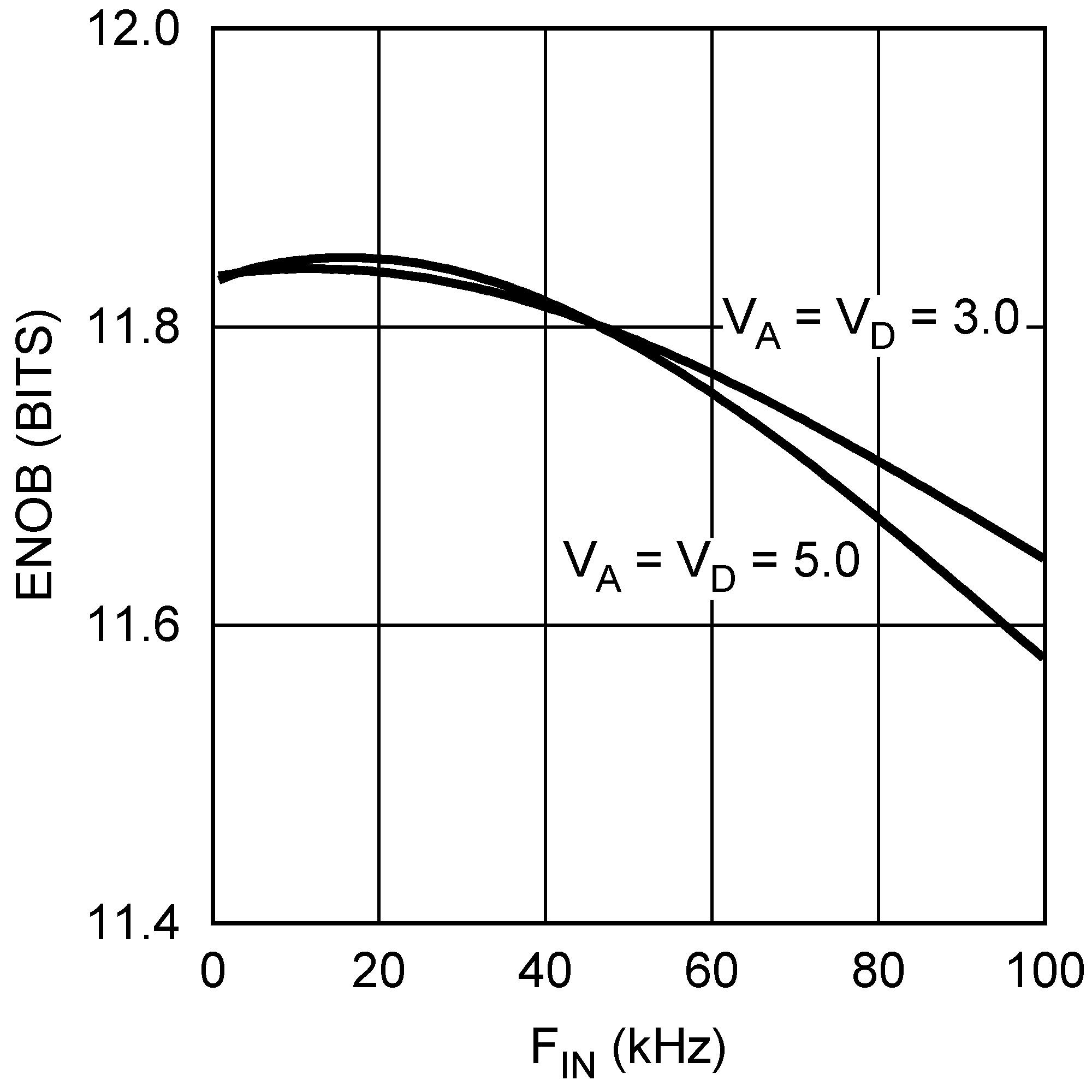 Figure 39. Typical Performance