SNAS298G August 2005 – January 2015 ADC128S102
PRODUCTION DATA.
- 1 Features
- 2 Applications
- 3 Description
- 4 Revision History
- 5 Pin Configuration and Functions
- 6 Specifications
- 7 Detailed Description
- 8 Application and Implementation
- 9 Power Supply Recommendations
- 10Layout
- 11Device and Documentation Support
- 12Mechanical, Packaging, and Orderable Information
Package Options
Mechanical Data (Package|Pins)
- PW|16
Thermal pad, mechanical data (Package|Pins)
Orderable Information
11 Device and Documentation Support
11.1 Device Support
11.1.1 Specification Definitions
-
ACQUISITION TIME is the time required for the ADC to acquire the input voltage. During this time, the hold capacitor is charged by the input voltage.
-
APERTURE DELAY is the time between the fourth falling edge of SCLK and the time when the input signal is internally acquired or held for conversion.
-
CONVERSION TIMEis the time required, after the input voltage is acquired, for the ADC to convert the input voltage to a digital word.
-
CHANNEL-TO-CHANNEL ISOLATION is resistance to coupling of energy from one channel into another channel.
-
CROSSTALKis the coupling of energy from one channel into another channel. This is similar to Channel-to-Channel Isolation, except for the sign of the data.
-
DIFFERENTIAL NON-LINEARITY (DNL)is the measure of the maximum deviation from the ideal step size of 1 LSB.
-
DUTY CYCLEis the ratio of the time that a repetitive digital waveform is high to the total time of one period. The specification here refers to the SCLK.
-
EFFECTIVE NUMBER OF BITS (ENOB, or EFFECTIVE BITS) is another method of specifying Signal-to-Noise and Distortion or SINAD. ENOB is defined as (SINAD - 1.76) / 6.02 and says that the converter is equivalent to a perfect ADC of this (ENOB) number of bits.
-
FULL POWER BANDWIDTH is a measure of the frequency at which the reconstructed output fundamental drops 3 dB below its low frequency value for a full scale input.
-
FULL SCALE ERROR (FSE)
- Vmax is the voltage at which the transition to the maximum code occurs.
- FSE can be expressed in Volts, LSB or percent of full scale range.
is a measure of how far the last code transition is from the ideal 1½ LSB below VREF+ and is defined as:
Equation 7. VFSE = Vmax + 1.5 LSB – VREF+
where
-
GAIN ERROR is the deviation of the last code transition (111...110) to (111...111) from the ideal (VREF - 1.5 LSB), after adjusting for offset error.
-
INTEGRAL NON-LINEARITY (INL) is a measure of the deviation of each individual code from a line drawn from negative full scale (½ LSB below the first code transition) through positive full scale (½ LSB above the last code transition). The deviation of any given code from this straight line is measured from the center of that code value.
-
INTERMODULATION DISTORTION (IMD) is the creation of additional spectral components as a result of two sinusoidal frequencies being applied to an individual ADC input at the same time. It is defined as the ratio of the power in both the second or the third order intermodulation products to the power in one of the original frequencies. Second order products are fa ± fb, where fa and fb are the two sine wave input frequencies. Third order products are (2fa ± fb ) and (fa ± 2fb). IMD is usually expressed in dB.
-
MISSING CODES are those output codes that will never appear at the ADC outputs. These codes cannot be reached with any input value. The ADC128S102 is ensured not to have any missing codes.
-
OFFSET ERRORis the deviation of the first code transition (000...000) to (000...001) from the ideal (i.e. GND + 0.5 LSB).
-
SIGNAL TO NOISE PLUS DISTORTION (S/N+D or SINAD) is the ratio, expressed in dB, of the rms value of the input signal to the rms value of all of the other spectral components below half the clock frequency, including harmonics but excluding d.c.
-
SIGNAL TO NOISE RATIO (SNR) is the ratio, expressed in dB, of the rms value of the input signal to the rms value of the sum of all other spectral components below one-half the sampling frequency, not including d.c. or the harmonics included in THD.
-
SPURIOUS FREE DYNAMIC RANGE (SFDR)is the difference, expressed in dB, between the desired signal amplitude to the amplitude of the peak spurious spectral component, where a spurious spectral component is any signal present in the output spectrum that is not present at the input and may or may not be a harmonic.
-
THROUGHPUT TIME is the minimum time required between the start of two successive conversions. It is the acquisition time plus the conversion and read out times. In the case of the ADC128S102, this is 16 SCLK periods.
-
TOTAL HARMONIC DISTORTION (THD) is the ratio, expressed in dBc, of the rms total of the first five harmonic components at the output to the rms level of the input signal frequency as seen at the output. THD is calculated as:
- Af1 is the RMS power of the input frequency at the output
- Af2 through Af10 are the RMS power in the first 9 harmonic frequencies
Equation 8. 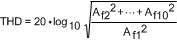
where
11.2 Trademarks
QSPI is a trademark of Motorola, Inc..
MICROWIRE is a trademark of TI.
All other trademarks are the property of their respective owners.
11.3 Electrostatic Discharge Caution

These devices have limited built-in ESD protection. The leads should be shorted together or the device placed in conductive foam during storage or handling to prevent electrostatic damage to the MOS gates.
11.4 Glossary
SLYZ022 — TI Glossary.
This glossary lists and explains terms, acronyms, and definitions.