SNAS298G August 2005 – January 2015 ADC128S102
PRODUCTION DATA.
- 1 Features
- 2 Applications
- 3 Description
- 4 Revision History
- 5 Pin Configuration and Functions
- 6 Specifications
- 7 Detailed Description
- 8 Application and Implementation
- 9 Power Supply Recommendations
- 10Layout
- 11Device and Documentation Support
- 12Mechanical, Packaging, and Orderable Information
Package Options
Mechanical Data (Package|Pins)
- PW|16
Thermal pad, mechanical data (Package|Pins)
Orderable Information
5 Pin Configuration and Functions
PW Package
16-Pin TSSOP
Top View
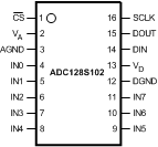
Pin Functions
| PIN | I/O | DESCRIPTION | |
|---|---|---|---|
| NO. | NAME | ||
| 3 | AGND | Supply | The ground return for the analog supply and signals. |
| 1 | CS | IN | Chip select. On the falling edge of CS, a conversion process begins. Conversions continue as long as CS is held low. |
| 12 | DGND | Supply | The ground return for the digital supply and signals. |
| 14 | DIN | IN | Digital data input. The ADC128S102's Control Register is loaded through this pin on rising edges of the SCLK pin. |
| 15 | DOUT | OUT | Digital data output. The output samples are clocked out of this pin on the falling edges of the SCLK pin. |
| 4 - 11 | IN0 to IN7 | IN | Analog inputs. These signals can range from 0 V to VREF. |
| 16 | SCLK | IN | Digital clock input. The ensured performance range of frequencies for this input is 8 MHz to 16 MHz. This clock directly controls the conversion and readout processes. |
| 2 | VA | Supply | Positive analog supply pin. This voltage is also used as the reference voltage. This pin should be connected to a quiet +2.7-V to +5.25-V source and bypassed to GND with 1-µF and 0.1-µF monolithic ceramic capacitors located within 1 cm of the power pin. |
| 13 | VD | Supply | Positive digital supply pin. This pin should be connected to a +2.7 V to VA supply, and bypassed to GND with a 0.1-µF monolithic ceramic capacitor located within 1 cm of the power pin. |