SBAS860 August 2017 ADC31RF80
PRODUCTION DATA.
- 1 Features
- 2 Applications
- 3 Description
- 4 Revision History
- 5 Pin Configuration and Functions
-
6 Specifications
- 6.1 Absolute Maximum Ratings
- 6.2 ESD Ratings
- 6.3 Recommended Operating Conditions
- 6.4 Thermal Information
- 6.5 Electrical Characteristics
- 6.6 AC Performance Characteristics: fS = 2949.12 MSPS
- 6.7 AC Performance Characteristics: fS = 2457.6 MSPS (Performance Optimized for F + A + D Band)
- 6.8 AC Performance Characteristics: fS = 2457.6 MSPS (Performance Optimized for F + A Band)
- 6.9 Digital Requirements
- 6.10 Timing Requirements
- 6.11 Typical Characteristics
- 7 Parameter Measurement Information
-
8 Detailed Description
- 8.1 Overview
- 8.2 Functional Block Diagram
- 8.3
Feature Description
- 8.3.1 Analog Inputs
- 8.3.2 Clock Input
- 8.3.3 SYSREF Input
- 8.3.4 DDC Block
- 8.3.5 NCO Switching
- 8.3.6 SerDes Transmitter Interface
- 8.3.7 Eye Diagrams
- 8.3.8 Alarm Outputs: Power Detectors for AGC Support
- 8.3.9 Power-Down Mode
- 8.3.10 ADC Test Pattern
- 8.4
Device Functional Modes
- 8.4.1 Device Configuration
- 8.4.2
JESD204B Interface
- 8.4.2.1 JESD204B Initial Lane Alignment (ILA)
- 8.4.2.2 JESD204B Frame Assembly
- 8.4.2.3 JESD204B Frame Assembly with Decimation (Single-Band DDC): Complex Output
- 8.4.2.4 JESD204B Frame Assembly with Decimation (Single-Band DDC): Real Output
- 8.4.2.5 JESD204B Frame Assembly with Decimation (Single-Band DDC): Real Output
- 8.4.2.6 JESD204B Frame Assembly with Decimation (Dual-Band DDC): Complex Output
- 8.4.2.7 JESD204B Frame Assembly with Decimation (Dual-Band DDC): Real Output
- 8.4.3 Serial Interface
- 8.5
Register Maps
- 8.5.1 Example Register Writes
- 8.5.2
Register Descriptions
- 8.5.2.1
General Registers
- 8.5.2.1.1 Register 000h (address = 000h), General Registers
- 8.5.2.1.2 Register 002h (address = 002h), General Registers
- 8.5.2.1.3 Register 003h (address = 003h), General Registers
- 8.5.2.1.4 Register 004h (address = 004h), General Registers
- 8.5.2.1.5 Register 010h (address = 010h), General Registers
- 8.5.2.1.6 Register 011h (address = 011h), General Registers
- 8.5.2.1.7 Register 012h (address = 012h), General Registers
- 8.5.2.1
General Registers
- 8.5.3
Master Page (M = 0)
- 8.5.3.1 Register 020h (address = 020h), Master Page
- 8.5.3.2 Register 032h (address = 032h), Master Page
- 8.5.3.3 Register 039h (address = 039h), Master Page
- 8.5.3.4 Register 03Ch (address = 03Ch), Master Page
- 8.5.3.5 Register 05Ah (address = 05Ah), Master Page
- 8.5.3.6 Register 03Dh (address = 3Dh), Master Page
- 8.5.3.7 Register 057h (address = 057h), Master Page
- 8.5.3.8 Register 058h (address = 058h), Master Page
- 8.5.4 ADC Page (FFh, M = 0)
- 8.5.5 Digital Function Page (610000h, M = 1)
- 8.5.6 Offset Corr Page (610000h, M = 1)
- 8.5.7 Digital Gain Page (610005h, M = 1)
- 8.5.8
Main Digital Page (680000h, M = 1)
- 8.5.8.1 Register 000h (address = 000h), Main Digital Page
- 8.5.8.2 Register 0A2h (address = 0A2h), Main Digital Page
- 8.5.8.3 Register 0A5h (address = 0A5h), Main Digital Page
- 8.5.8.4 Register 0A9h (address = 0A9h), Main Digital Page
- 8.5.8.5 Register 0B0h (address = 0B0h), Main Digital Page
- 8.5.8.6 Register 0B1h (address = 0B1h), Main Digital Page
- 8.5.8.7 Register 0B2h (address = 0B2h), Main Digital Page
- 8.5.8.8 Register 0B3h (address = 0B3h), Main Digital Page
- 8.5.8.9 Register 0B4h (address = 0B4h), Main Digital Page
- 8.5.8.10 Register 0B5h (address = 0B5h), Main Digital Page
- 8.5.8.11 Register 0B6h (address = 0B6h), Main Digital Page
- 8.5.8.12 Register 0B7h (address = 0B7h), Main Digital Page
- 8.5.8.13 Register 0B8h (address = 0B8h), Main Digital Page
- 8.5.8.14 Register 0B9h (address = 0B9h), Main Digital Page
- 8.5.8.15 Register 0BAh (address = 0BAh), Main Digital Page
- 8.5.8.16 Register 0BBh (address = 0BBh), Main Digital Page
- 8.5.9
JESD Digital Page (6900h, M = 1)
- 8.5.9.1 Register 001h (address = 001h), JESD Digital Page
- 8.5.9.2 Register 002h (address = 002h ), JESD Digital Page
- 8.5.9.3 Register 003h (address = 003h), JESD Digital Page
- 8.5.9.4 Register 004h (address = 004h), JESD Digital Page
- 8.5.9.5 Register 006h (address = 006h), JESD Digital Page
- 8.5.9.6 Register 007h (address = 007h), JESD Digital Page
- 8.5.9.7 Register 016h (address = 016h), JESD Digital Page
- 8.5.9.8 Register 017h (address = 017h), JESD Digital Page
- 8.5.9.9 Register 032h-035h (address = 032h-035h), JESD Digital Page
- 8.5.9.10 Register 036h (address = 036h), JESD Digital Page
- 8.5.9.11 Register 037h (address = 037h), JESD Digital Page
- 8.5.9.12 Register 03Ch (address = 03Ch), JESD Digital Page
- 8.5.9.13 Register 03Eh (address = 03Eh), JESD Digital Page
- 8.5.10
Decimation Filter Page
- 8.5.10.1 Register 000h (address = 000h), Decimation Filter Page
- 8.5.10.2 Register 001h (address = 001h), Decimation Filter Page
- 8.5.10.3 Register 002h (address = 2h), Decimation Filter Page
- 8.5.10.4 Register 005h (address = 005h), Decimation Filter Page
- 8.5.10.5 Register 007h (address = 007h), Decimation Filter Page
- 8.5.10.6 Register 008h (address = 008h), Decimation Filter Page
- 8.5.10.7 Register 009h (address = 009h), Decimation Filter Page
- 8.5.10.8 Register 00Ah (address = 00Ah), Decimation Filter Page
- 8.5.10.9 Register 00Bh (address = 00Bh), Decimation Filter Page
- 8.5.10.10 Register 00Ch (address = 00Ch), Decimation Filter Page
- 8.5.10.11 Register 00Dh (address = 00Dh), Decimation Filter Page
- 8.5.10.12 Register 00Eh (address = 00Eh), Decimation Filter Page
- 8.5.10.13 Register 00Fh (address = 00Fh), Decimation Filter Page
- 8.5.10.14 Register 010h (address = 010h), Decimation Filter Page
- 8.5.10.15 Register 011h (address = 011h), Decimation Filter Page
- 8.5.10.16 Register 014h (address = 014h), Decimation Filter Page
- 8.5.10.17 Register 016h (address = 016h), Decimation Filter Page
- 8.5.10.18 Register 01Eh (address = 01Eh), Decimation Filter Page
- 8.5.10.19 Register 01Fh (address = 01Fh), Decimation Filter Page
- 8.5.10.20 Register 033h-036h (address = 033h-036h), Decimation Filter Page
- 8.5.10.21 Register 037h (address = 037h), Decimation Filter Page
- 8.5.10.22 Register 038h (address = 038h), Decimation Filter Page
- 8.5.10.23 Register 039h (address = 039h), Decimation Filter Page
- 8.5.10.24 Register 03Ah (address = 03Ah), Decimation Filter Page
- 8.5.11
Power Detector Page
- 8.5.11.1 Register 000h (address = 000h), Power Detector Page
- 8.5.11.2 Register 001h-002h (address = 001h-002h), Power Detector Page
- 8.5.11.3 Register 003h (address = 003h), Power Detector Page
- 8.5.11.4 Register 007h-00Ah (address = 007h-00Ah), Power Detector Page
- 8.5.11.5 Register 00Bh-00Ch (address = 00Bh-00Ch), Power Detector Page
- 8.5.11.6 Register 00Dh (address = 00Dh), Power Detector Page
- 8.5.11.7 Register 00Eh (address = 00Eh), Power Detector Page
- 8.5.11.8 Register 00Fh, 010h-012h, and 016h-019h (address = 00Fh, 010h-012h, and 016h-019h), Power Detector Page
- 8.5.11.9 Register 013h-01Ah (address = 013h-01Ah), Power Detector Page
- 8.5.11.10 Register 01Dh-01Eh (address = 01Dh-01Eh), Power Detector Page
- 8.5.11.11 Register 020h (address = 020h), Power Detector Page
- 8.5.11.12 Register 021h (address = 021h), Power Detector Page
- 8.5.11.13 Register 022h-025h (address = 022h-025h), Power Detector Page
- 8.5.11.14 Register 027h (address = 027h), Power Detector Page
- 8.5.11.15 Register 02Bh (address = 02Bh), Power Detector Page
- 8.5.11.16 Register 032h-035h (address = 032h-035h), Power Detector Page
- 8.5.11.17 Register 037h (address = 037h), Power Detector Page
- 8.5.11.18 Register 038h (address = 038h), Power Detector Page
- 9 Application and Implementation
- 10Power Supply Recommendations
- 11Layout
- 12Device and Documentation Support
- 13Mechanical, Packaging, and Orderable Information
Package Options
Mechanical Data (Package|Pins)
- RMP|72
Thermal pad, mechanical data (Package|Pins)
Orderable Information
8 Detailed Description
8.1 Overview
The ADC31RF80 is a single-channel, 14-bit, 2949.12-MSPS, telecom receiver and feedback device containing an analog-to-digital converter (ADC) followed by multi-band digital down-converters (DDCs), and a back-end JESD204B digital interface.
The ADC is preceded by an input buffer and on-chip termination to provide a uniform input impedance over a large input frequency range. Furthermore, an internal differential clamping circuit provides first-level protection against overvoltage conditions. The ADC is internally interleaved four times and equipped with background, analog and digital, and interleaving correction.
The on-chip DDC enables single- or dual-band internal processing to pre-select and filter smaller bands of interest and also reduces the digital output data traffic. Each DDC is equipped with up to three independent,
16-bit numerically-controlled oscillators (NCOs) for phase coherent frequency hopping; the NCOs can be controlled through the SPI or GPIO pins. The ADC31RF80 also provides three different power detectors on-chip with alarm outputs in order to support external automatic gain control (AGC) loops.
The processed data are passed into the JESD204B interface where the data are framed, encoded, serialized, and output on one to four lanes, depending on the ADC sampling rate and decimation. The CLKIN, SYSREF, and SYNCB inputs provide the device clock and the SYSREF and SYNCB signals to the JESD204B interface that are used to derive the internal local frame and local multiframe clocks and establish the serial link. All features of the ADC31RF80 are configurable through the SPI.
8.2 Functional Block Diagram
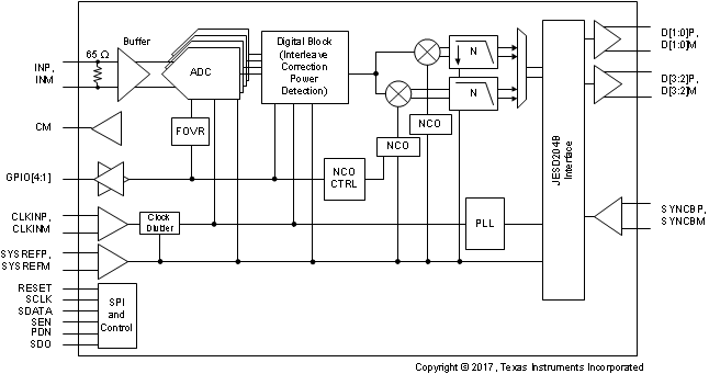
8.3 Feature Description
8.3.1 Analog Inputs
The ADC31RF80 analog signal inputs are designed to be driven differentially. The analog input pins have internal analog buffers that drive the sampling circuit. The ADC31RF80 provides on-chip, differential termination to minimize reflections. The buffer also helps isolate the external driving circuit from the internal switching currents of the sampling circuit, thus resulting in a more constant SFDR performance across input frequencies.
The common-mode voltage of the signal inputs is internally biased to CM using the 32.5-Ω termination resistors that allow for ac-coupling of the input drive network. Figure 80 and Figure 81 show SDD11 at the analog inputs from dc to 5 GHz with a 100-Ω reference impedance.
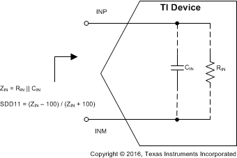
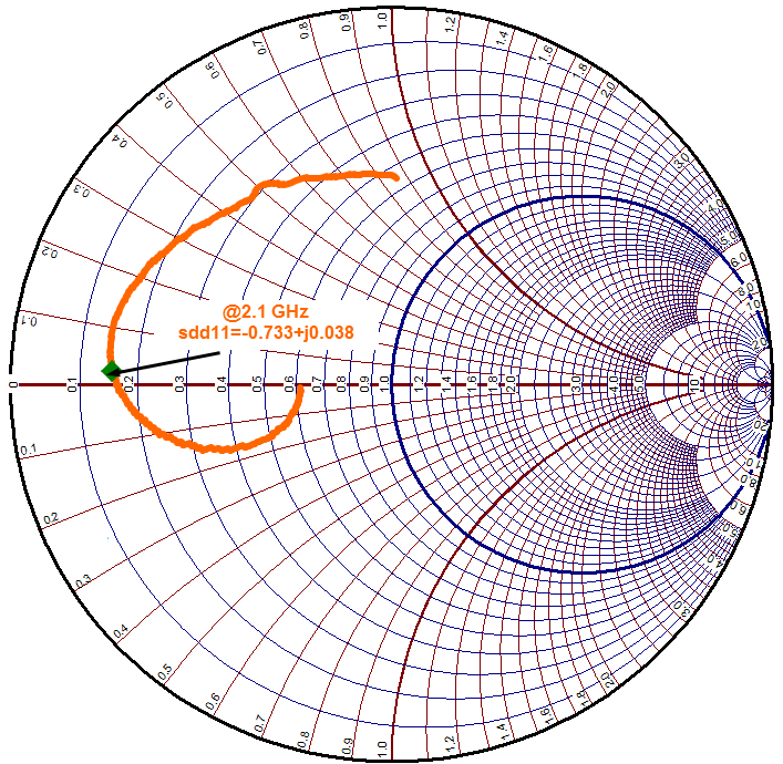 Figure 81. SDD11 Over the Input Frequency Range
The input impedance of analog inputs can also be modelled as parallel combination of equivalent resistance and capacitance. Figure 82 and Figure 83 show how equivalent impedance (CIN and RIN) vary over frequency.
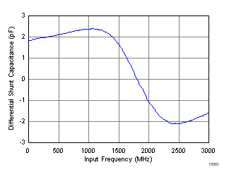 Figure 82. Differential Input Capacitance vs
 Input Frequency
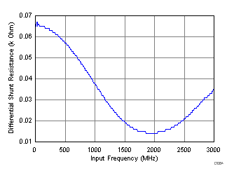 Figure 83. Differential Input Resistance vs Input Frquency
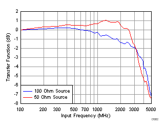
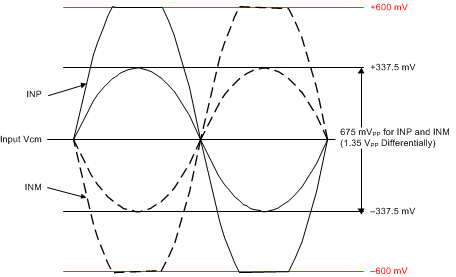
Each input pin (INP, INM) must swing symmetrically between (CM + 0.3375 V) and (CM – 0.3375 V), resulting in a 1.35-VPP (default) differential input swing. Figure 84 shows that the input sampling circuit has a 3-dB bandwidth that extends up to approximately 3.2 GHz.
8.3.1.1 Input Clamp Circuit
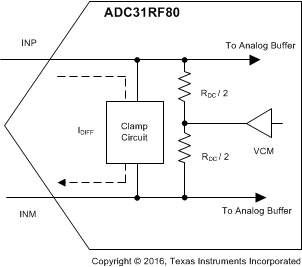
The ADC31RF80 analog inputs include an internal, differential clamp for overvoltage protection. The clamp triggers for any input signals at approximately 600 mV above the input common-mode voltage, as shown in Figure 85 and Figure 86, effectively limiting the maximum input signal to approximately 2.4 VPP.
When the clamp circuit conducts, the maximum differential current flowing through the circuit (via input pins) must be limited to 20 mA.
8.3.2 Clock Input
The ADC31RF80 sampling clock input includes internal 100-Ω differential termination along with on-chip biasing. The clock input is recommended to be ac-coupled externally. The input bandwidth of the clock input is approximately 3 GHz; Figure 87 shows the clock input impedance with a 100-Ω reference impedance.
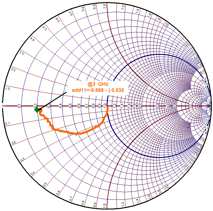 Figure 87. SDD11 of the Clock Input
The analog-to-digital converter (ADC) aperture jitter is a function of the clock amplitude applied to the pins. Figure 88 shows the equivalent aperture jitter for input frequencies at a 1-GHz and a 2-GHz input. Depending on the clock frequency, a matching circuit can be designed in order to maximize the clock amplitude.
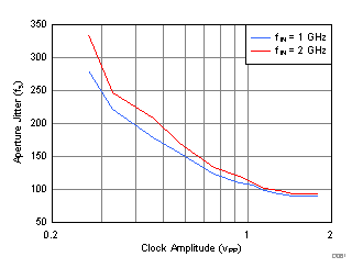 Figure 88. Equivalent Aperture Jitter vs Input Clock Amplitude
8.3.3 SYSREF Input
The SYSREF signal is a periodic signal that is sampled by the ADC31RF80 device clock and is used to align the boundary of the local multiframe clock inside the data converter. SYSREF is also used to reset critical blocks [such as the clock divider for the interleaved ADCs, numerically-controlled oscillators (NCOs), decimation filters and so forth].
The SYSREF input requires external biasing. Furthermore, SYSREF must be established before the SPI registers are programmed. A programmable delay on the SYSREF input, as shown in Figure 89, is available to help with skew adjustment when the sampling clock and SYSREF are not provided from the same source.
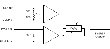 Figure 89. SYSREF Internal Circuit Diagram
8.3.3.1 Using SYSREF
The ADC31RF80 uses SYSREF information to reset the clock divider, the NCO phase, and the LMFC counter of the JESD interface. The device provides flexibility to provide SYSREF information either from dedicated pins or through SPI register bits. SYSREF is asserted by a low-to-high transition on the SYSREF pins or a 0-to-1 change in the ASSERT SYSREF REG bit, as shown in Figure 90, when using SPI registers.
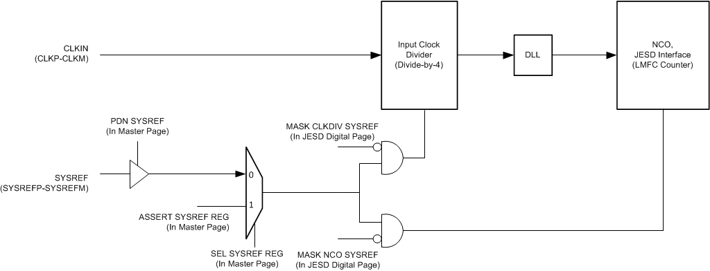 Figure 90. Using SYSREF to Reset the Clock Divider, the NCO, and the LMFC Counter
The ADC31RF80 samples the SYSREF signal on the input clock rising edge. Required setup and hold time are listed in the Timing Requirements table. The input clock divider gets reset each time that SYSREF is asserted, as shown in Table 1, whereas the NCO phase and the LMFC counter of the JESD interface are reset on each SYSREF assertion after disregarding the first two assertions.
Table 1. Asserting SYSREF
| SYSREF ASSERTION INDEX | ACTION | ||
|---|---|---|---|
| INPUT CLOCK DIVIDER | NCO PHASE | LMFC COUNTER | |
| 1 | Gets reset | Does not get reset | Does not get reset |
| 2 | Gets reset | Does not get reset | Does not get reset |
| 3 | Gets reset | Gets reset | Gets reset |
| 4 and onwards | Gets reset | Gets reset | Gets reset |
The SESREF use-cases can be classified broadly into two categories:
- SYSREF is applied as aperiodic multi-shot pulses.
- SYSREF is applied as a periodic pulse.
Figure 91 shows a case when only a counted number of pulses are applied as SYSREF to the ADC.
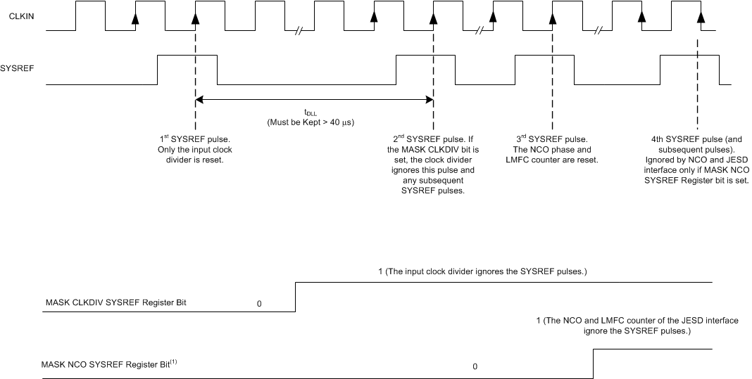
After the first SYSREF pulse is applied, allow the DLL in the clock path to settle by waiting for the tDLL time (> 40 µs) before applying the second pulse. During this time, mask the SYSREF going to the input clock divider by setting the MASK CLKDIV SYSREF bit so that the divider output phase remains stable. The NCO phase and LMFC counter are reset on the third SYSREF pulse. After the third SYSREF pulse, the SYSREF going to the NCO and JESD block can be disabled by setting the MASK NCO SYSREF bit to avoid any unwanted resets.
Figure 92 shows how SYSREF can be applied as a continuous periodic waveform.
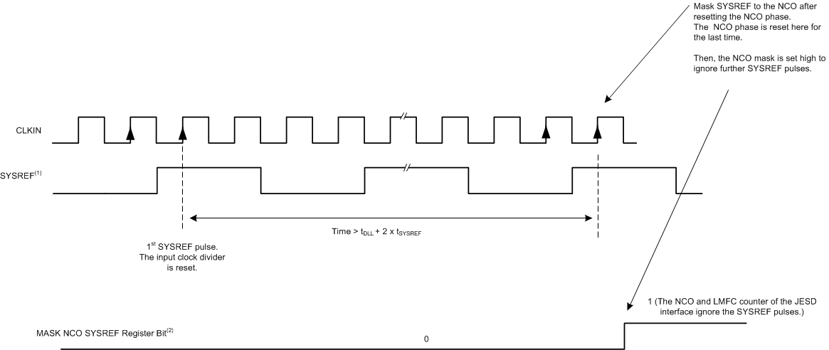
After applying the SYSREF signal, DLL must be allowed to lock, and the NCO phase and LMFC counter must be allowed to reset by waiting for at least the tDLL (40 µs) + 2 × tSYSREF time. Then, the SYSREF going to the NCO and JESD can be masked by setting the MASK NCO SYSREF register bit.
8.3.3.2 Frequency of the SYSREF Signal
When SYSREF is a periodic signal, as described in Equation 1, its frequency is required to be a sub-harmonic of the internal local multi-frame clock (LMFC) frequency. The LMFC frequency is determined by the selected decimation, frames per multi-frame setting (K), samples per frame (S), and device input clock frequency.
where
- N is an integer value (1, 2, 3, and so forth)
In order for the interleaving correction engine to synchronize properly, the SYSREF frequency must also be a multiple of fS / 64. Table 2 provides a summary of the valid LMFC clock settings.
Table 2. . SYSREF and LMFC Clock Frequency
| OPERATING MODE | LMFS SETTING | LMFC CLOCK FREQUENCY | SYSREF FRQUENCY |
|---|---|---|---|
| Decimation | Various | fS(1) / (D × S(4) × K(3)) | fS / (N × LCM(2) (64, D(5) × S × K)) |
The SYSREF signal is recommended to be a low-frequency signal less than 5 MHz in order to reduce coupling to the signal path both on the printed circuit board (PCB) as well as internal to the device.
Example: fS = 2949.12 MSPS, Divide-by-4 (LMFS = 8411), K = 16
SYSREF = 2949.12 MSPS / LCM (4 ,64, 16) = 46.08 MHz / N
Operate SYSREF at 2.88 MHz (effectively divide-by-1024, N = 16)
For proper device operation, disable the SYSREF signal after the JESD synchronization is established.
8.3.4 DDC Block
The ADC31RF80 provides a sophisticated on-chip, digital down converter (DDC) block that can be controlled through SPI register settings and the general-purpose input/output (GPIO) pins. The DDC block supports two basic operating modes: receiver (RX) mode with single- or dual-band DDC and wide-bandwidth observation receiver mode.
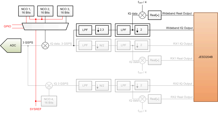
Figure 93 shows that the ADC channel is followed by two DDC chains consisting of the digital filter along with a complex digital mixer with a 16-bit numerically-controlled oscillator (NCO). The NCOs allow accurate frequency tuning within the Nyquist zone prior to the digital filtering. One DDC chain is intended for supporting a dual-band DDC configuration in receiver mode and the second DDC chain supports the wide-bandwidth output option for the observation configuration. At any given time, either the single-band DDC, the dual-band DDC, or the wideband DDC can be enabled. Furthermore, three different NCO frequencies can be selected on that path and are quickly switched using the SPI or the GPIO pins to enable wide-bandwidth observation in a multi-band application.
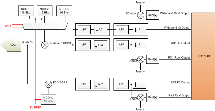
NOTE:
Red traces show SYSREF going to the NCO blocks.Additionally, the decimation filter block provides the option to convert the complex output back to real format at twice the decimated, complex output rate. The filter response with a real output is identical to a complex output. The band is centered in the middle of the Nyquist zone (mixed with fOUT / 4) based on a final output data rate of fOUT.
8.3.4.1 Operating Mode: Receiver
Figure 94 shows that the DDC block can be configured to single- or dual-band operation in receiver mode. Both DDC chains use the same decimation filter setting and the available options are discussed in the Decimation Filters section. The decimation filter setting also directly affects the interface rate and number of lanes of the JESD204B interface.
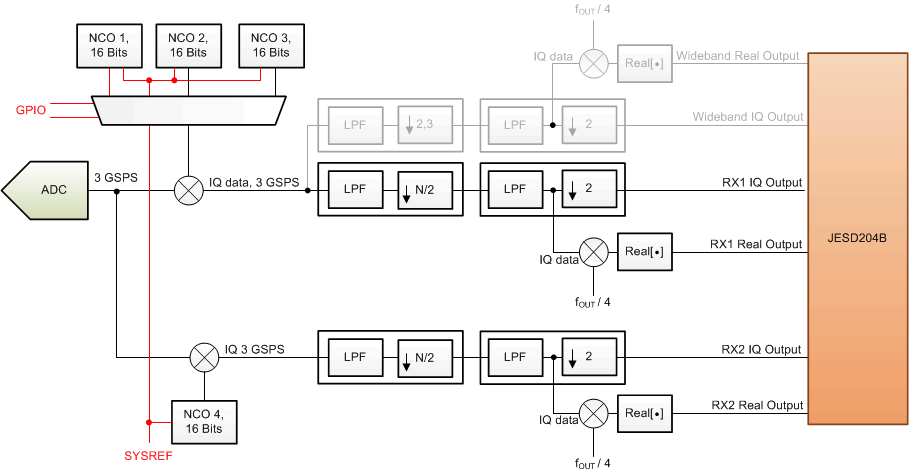
NOTE:
Red traces show SYSREF going to the NCO blocks.8.3.4.2 Operating Mode: Wide-Bandwidth Observation Receiver
This mode is intended for using a DDC with a wide bandwidth output, but for multiple bands. As shown in Figure 95, this mode uses a single DDC chain where up to three NCOs can be used to perform wide-bandwidth observation in a multi-band environment. The three NCOs can be switched dynamically using either the GPIO pins or an SPI command. All three NCOs operate continuously to ensure phase continuity; however, when the NCO is switched, the output data are invalid until the decimation filters are completely flushed with data from the new band.
NOTE:
Red traces show SYSREF going to the NCO blocks.8.3.4.3 Decimation Filters
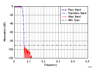
The stop-band rejection of the decimation filters is approximately 90 dB with a pass-band bandwidth of approximately 80%. Table 3 gives an overview of the pass-band bandwidth depending on decimation filter setting and ADC sampling rate.
Table 3. Decimation Filter Summary and Maximum Available Output Bandwidth
| DECIMATION SETTING | NO. OF DDCS | NOMINAL PASSBAND GAIN | BANDWIDTH | ADC SAMPLE RATE = N MSPS | ADC SAMPLE RATE = 3 GSPS | |||
|---|---|---|---|---|---|---|---|---|
| 3 dB (%) | 1 dB (%) | OUTPUT RATE (MSPS) PER BAND | OUTPUT BANDWIDTH (MHz) PER BAND | COMPLEX OUTPUT RATE (MSPS) PER BAND | OUTPUT BANDWIDTH (MHz) PER BAND | |||
| Divide-by-4 complex | 1 | –0.4 dB | 90.9 | 86.8 | N / 4 complex | 0.4 × N / 2 | 750 | 600 |
| Divide-by-6 complex | 1 | –0.65 dB | 90.6 | 86.1 | N / 6 complex | 0.4 × N / 3 | 500 | 400 |
| Divide-by-8 complex | 2 | –0.27 dB | 91.0 | 86.8 | N / 8 complex | 0.4 × N / 4 | 375 | 300 |
| Divide-by-9 complex | 2 | –0.45 dB | 90.7 | 86.3 | N / 9 complex | 0.4 × N / 4.5 | 333.3 | 266.6 |
| Divide-by-10 complex | 2 | –0.58 dB | 90.7 | 86.3 | N / 10 complex | 0.4 × N / 5 | 300 | 240 |
| Divide-by-12 complex | 2 | –0.55 dB | 90.7 | 86.4 | N / 12 complex | 0.4 × N / 6 | 250 | 200 |
| Divide-by-16 complex | 2 | –0.42 dB | 90.8 | 86.4 | N / 16 complex | 0.4 × N / 8 | 187.5 | 150 |
| Divide-by-18 complex | 2 | –0.83 dB | 91.2 | 87.0 | N / 18 complex | 0.4 × N / 9 | 166.6 | 133 |
| Divide-by-20 complex | 2 | –0.91 dB | 91.2 | 87.0 | N / 20 complex | 0.4 × N / 10 | 150 | 120 |
| Divide-by-24 complex | 2 | –0.95 db | 91.1 | 86.9 | N / 24 complex | 0.4 × N / 12 | 125 | 100 |
| Divide-by-32 complex | 2 | –0.78 dB | 91.1 | 86.8 | N / 32 complex | 0.4 × N / 16 | 93.75 | 75 |
Figure 96 shows a dual-band example with a divide-by-8 complex.
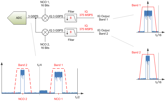 Figure 96. Dual-Band Example
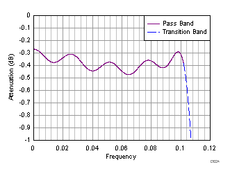
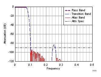
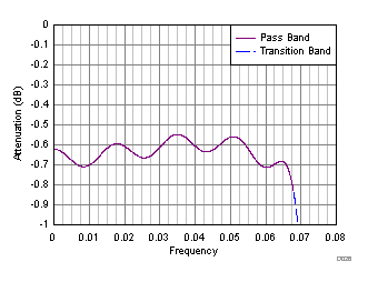
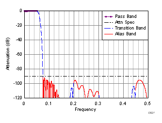
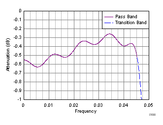
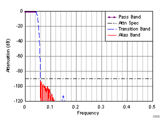
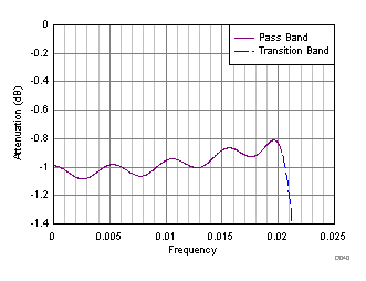
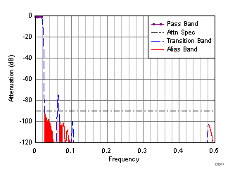
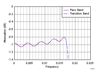
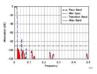
The decimation filter responses normalized to the ADC sampling clock are illustrated in Figure 96 to Figure 119 and can be interpreted as follows:
Figure 97 shows that each figure contains the filter pass-band, transition bands, and alias bands. The x-axis in Figure 97 shows the offset frequency (after the NCO frequency shift) normalized to the ADC sampling clock frequency.
For example, in the divide-by-4 complex, the output data rate is an fS / 4 complex with a Nyquist zone of fS / 8 or 0.125 × fS. The transition band is centered around 0.125 × fS and the alias transition band is centered at 0.375 × fS. The alias bands that alias on top of the wanted signal band are centered at 0.25 × fS and 0.5 × fS (and are colored in red).
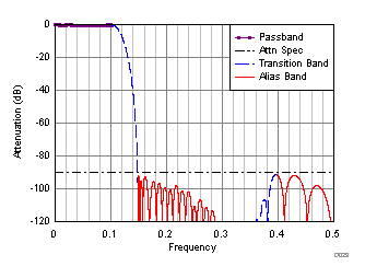
The decimation filters of the ADC31RF80 provide greater than 90-dB attenuation for the alias bands.
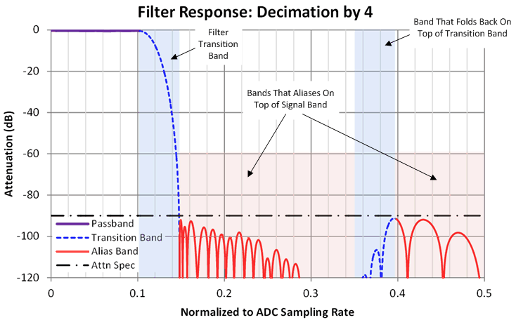 Figure 97. Interpretation of the Decimation Filter Plots
8.3.4.3.1 Divide-by-4
Peak-to-peak pass-band ripple: approximately 0.22 dB
8.3.4.3.2 Divide-by-6
Peak-to-peak pass-band ripple: approximately 0.38 dB
8.3.4.3.3 Divide-by-8
Peak-to-peak pass-band ripple: approximately 0.25 dB
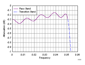
8.3.4.3.4 Divide-by-9
Peak-to-peak pass-band ripple: approximately 0.39 dB
8.3.4.3.5 Divide-by-10
Peak-to-peak pass-band ripple: approximately 0.39 dB
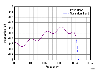
8.3.4.3.6 Divide-by-12
Peak-to-peak pass-band ripple: approximately 0.36 dB
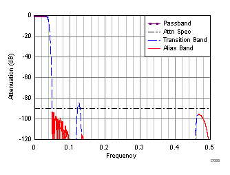
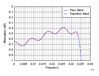
8.3.4.3.7 Divide-by-16
Peak-to-peak pass-band ripple: approximately 0.29 dB
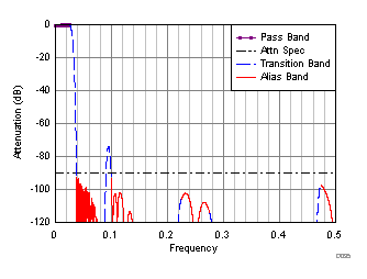
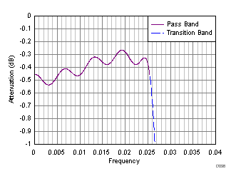
8.3.4.3.8 Divide-by-18
Peak-to-peak pass-band ripple: approximately 0.33 dB
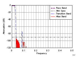
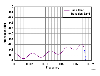
8.3.4.3.9 Divide-by-20
Peak-to-peak pass-band ripple: approximately 0.32 dB
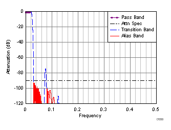
8.3.4.3.10 Divide-by-24
Peak-to-peak pass-band ripple: approximately 0.30 dB
8.3.4.3.11 Divide-by-32
Peak-to-peak pass-band ripple: approximately 0.24 dB
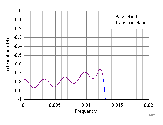
8.3.4.3.12 Latency With Decimation Options
Table 4 describes device latency for different DDC options. At higher decimation options, latency increases because of the increase in number of taps in the decimation filter.
Table 4. Latency With Different Decimation Options
| DECIMATION OPTION | TOTAL LATENCY, DEVICE CLOCK CYCLES |
|---|---|
| Divide-by-4 | 516 |
| Divide-by-6 | 746 |
| Divide-by-8 | 621 |
| Divide-by-9 | 763.5 |
| Divide-by-10 | 811 |
| Divide-by-12 | 897 |
| Divide-by-16 | 1045 |
| Divide-by-18 | 1164 |
| Divide-by-20 | 1256 |
| Divide-by-24 | 1443 |
| Divide-by-32 | 1773 |
8.3.4.4 Numerically-Controlled Oscillators (NCOs) and Mixers
The ADC31RF80 is equipped with three independent, complex NCOs. Equation 2 shows how the oscillator generates a complex exponential sequence.
where
- frequency (ω) is specified as a signed number by the 16-bit register setting
The complex exponential sequence is multiplied by the real input from the ADC to mix the desired carrier down to 0 Hz.
The ADC has two DDCs. The first DDC has three NCOs and the second DDC has one NCO. The first DDC can dynamically select one of the three NCOs based on the GPIO pin or SPI selection. In wide-bandwidth mode (lower decimation factors, for example, 4 and 6), there can only be one active DDC. The NCO frequencies can be programmed independently through the DDCx, NCO[4:1], and the MSB and LSB register settings.
Equation 3 gives the NCO frequency setting that is set by the 16-bit register:

where
- x = 0, 1
- y = 1 to 4
For example:
If fS = 2949.12 MSPS, then the NCO register setting = 38230 (decimal).
Thus, Equation 4 defines fNCO:

Any register setting changes that occur after the JESD204B interface is operational results in a non-deterministic NCO phase. If a deterministic phase is required, the JESD204B interface must be reinitialized after changing the register setting.
8.3.5 NCO Switching
The first DDC (DDC0) provides three different NCOs that can be used for phase-coherent frequency hopping. This feature is available in both single-band and dual-band mode, but only affects DDC0.
The NCOs can be switched by using the GPIO pins with the register configurations shown in Table 5 or through an SPI control. The assignment of which GPIO pin to use for INSEL0 and INSEL1 is done based on Table 6, using register 5438h. The NCO selection, shown in Table 7 and Figure 120, is done based on the logic selection on the GPIO pins.
Table 5. NCO Register Configurations
| REGISTER | ADDRESS | DESCRIPTION |
|---|---|---|
| NCO CONTROL THROUGH GPIO PINS | ||
| NCO SEL PIN | 500Fh | Selects the NCO control through the SPI (default) or a GPIO pin. |
| INSEL0[1:0], INSEL1[1:0] | 5438h | Selects which two GPIO pins are used to control the NCO. |
| NCO CONTROL THROUGH SPI CONTROL | ||
| NCO SEL PIN | 500Fh | Selects the NCO control through the SPI (default) or a GPIO pin. |
| NCO SEL[1:0] | 5010h | Selects which NCO to use for DDC0. |
Table 6. GPIO Pin Assignment
| INSELx[1:0] (Where x = 0 or 1) | GPIO PIN SELECTED |
|---|---|
| 00 | GPIO4 |
| 01 | GPIO1 |
| 10 | GPIO3 |
| 11 | GPIO2 |
Table 7. NCO Selection
| NCO SEL[1:0] | NCO SELECTED |
|---|---|
| 00 | NCO1 |
| 01 | NCO2 |
| 10 | NCO3 |
| 11 | n/a |
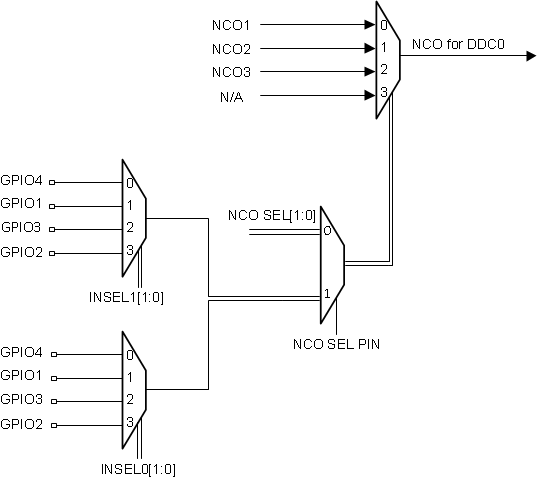 Figure 120. NCO Switching from GPIO and SPI
8.3.6 SerDes Transmitter Interface
Each 12.3-Gbps serializer, deserializer (SerDes) LVDS transmitter output requires ac-coupling between the transmitter and receiver. Terminate the differential pair, as shown in Figure 121, with 100-Ω resistance (that is, two 50-Ω resistors) as close to the receiving device as possible to avoid unwanted reflections and signal degradation.
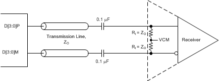 Figure 121. External Serial JESD204B Interface Connection
8.3.7 Eye Diagrams
Figure 122 and Figure 123 show the serial output eye diagrams of the ADC31RF80 at 5.0 Gbps and 12 Gbps against the JESD204B mask.
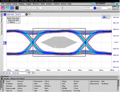 Figure 122. Data Eye at 5 Gbps
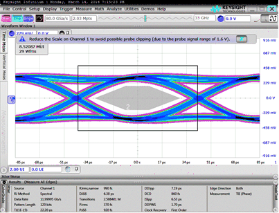 Figure 123. Data Eye at 12 Gbps
8.3.8 Alarm Outputs: Power Detectors for AGC Support
The GPIO pins can be configured as alarm outputs. The ADC31RF80 supports three different power detectors (an absolute peak power detector, crossing detector, and RMS power detector) as well as fast overrange from the ADC. The power detectors operate off the full-rate ADC output prior to the decimation filters.
8.3.8.1 Absolute Peak Power Detector
In this detector mode, the peak is computed over eight samples of the ADC output. Next, the peak for a block of N samples (N × S`) is computed over a programmable block length and then compared against a threshold to either set or reset the peak detector output (Figure 124 and Figure 125). There are two sets of thresholds and each set has two thresholds for hysteresis. The programmable DWELL-time counter is used for clearing the block detector alarm output.
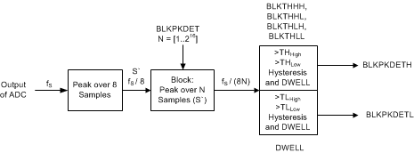 Figure 124. Peak Power Detector Implementation
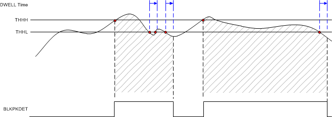 Figure 125. Peak Power Detector Timing Diagram
Table 8 shows the register configurations required to set up the absolute peak power detector. The detector operates in the fS / 8 clock domain; one peak sample is calculated over eight actual samples.
The automatic gain control (AGC) modes can be configured using registers in the power-detector page (54xxh).
Table 8. Registers Required for the Peak Power Detector
| REGISTER | ADDRESS | DESCRIPTION |
|---|---|---|
| PKDET EN | 5400h | Enables peak detector |
| BLKPKDET | 5401h, 5402h, 5403h | Sets the block length N of number of samples (S`). Number of actual ADC samples is 8x this value: N is 17 bits: 1 to 216. |
| BLKTHHH, BLKTHHL, BLKTHLH, BLKTHLL | 5407h, 5408h, 5409h, 540Ah | Sets the different thresholds for the hysteresis function values from 0 to 256 (where 256 is equivalent to the peak amplitude). For example: if BLKTHHH is to –2 dBFS from peak, 10(–2 / 20) × 256 = 203, then set 5407h = CBh. |
| DWELL | 540Bh, 540Ch | When the computed block peak crosses the upper thresholds BLKTHHH or BLKTHLH, the peak detector output flags are set. In order to be reset, the computed block peak must remain continuously lower than the lower threshold (BLKTHHL or BLKTHLL) for the period specified by the DWELL value. This threshold is 16 bits and is specified in terms of fS / 8 clock cycles. |
| OUTSEL GPIO[4:1] | 5432h, 5433h, 5434h, 5435h | Connects the BLKPKDETH, BLKPKDETL alarms to the GPIO pins; common register. |
| IODIR | 5437h | Selects the direction for the four GPIO pins; common register. |
| RESET AGC | 542Bh | After configuration, reset the AGC module to start operation. |
8.3.8.2 Crossing Detector
In this detector mode the peak is computed over eight samples of the ADC output. Next, the peak for a block of N samples (N × S`) is computed over a programmable block length and then the peak is compared against two sets of programmable thresholds (with hysteresis). The crossing detector counts how many fS / 8 clock cycles that the block detector outputs are set high over a programmable time period and compares the counter value against the programmable thresholds. Figure 126 and Figure 127 show that the alarm outputs are updated at the end of the time period, routed to the GPIO pins, and held in that state through the next cycle. Alternatively, a 2-bit format can be used but (because the ADC31RF80 has four GPIO pins available) this feature uses all four pins.
 Figure 126. Crossing Detector Implementation
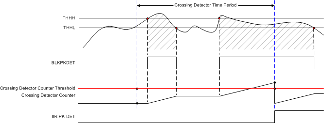 Figure 127. Crossing Detector Timing Diagram
Table 9 shows the register configurations required to set up the crossing detector. The detector operates in the
fS / 8 clock domain. The AGC modes can be configured through registers located in the power detector page (54xxh).
Table 9. Registers Required for the Crossing Detector Operation
| REGISTER | ADDRESS | DESCRIPTION |
|---|---|---|
| PKDET EN | 5400h | Enables peak detector |
| BLKPKDET | 5401h, 5402h, 5403h | Sets the block length N of number of samples (S`). Number of actual ADC samples is 8x this value: N is 17 bits: 1 to 216. |
| BLKTHHH, BLKTHHL, BLKTHLH, BLKTHLL | 5407h, 5408h, 5409h, 540Ah | Sets the different thresholds for the hysteresis function values from 0 to 256 (where 256 is equivalent to the peak amplitude). For example: if BLKTHHH is to –2 dBFS from peak, 10(–2 / 20) × 256 = 203, then set 5407h = CBh. |
| FILT0LPSEL | 540Dh | Select block detector output or 2-bit output mode as the input to the interrupt identification register (IIR) filter. |
| TIMECONST | 540Eh, 540Fh, | Sets the crossing detector time period for N = 0 to 15 as 2N × fS / 8 clock cycles. The maximum time period is 32768 × fS / 8 clock cycles (approximately 87 µs at 3 GSPS). |
| FIL0THH, FIL0THL, FIL1THH, FIL1THL | 540Fh-5412h, 5416h-5419h | Comparison thresholds for the crossing detector counter. These thresholds are 16-bit thresholds in 2.14-signed notation. A value of 1 (4000h) corresponds to 100% crossings, a value of 0.125 (0800h) corresponds to 12.5% crossings. |
| DWELLIIR | 541Dh, 541Eh | DWELL counter for the IIR filter hysteresis. |
| IIR0 2BIT EN, IIR1 2BIT EN |
5413h, 54114h | Enables 2-bit output format for the crossing detector. |
| OUTSEL GPIO[4:1] | 5432h, 5433h, 5434h, 5435h |
Connects the IIRPKDET0, IIRPKDET1 alarms to the GPIO pins; common register. |
| IODIR | 5437h | Selects the direction for the four GPIO pins; common register. |
| RESET AGC | 542Bh | After configuration, reset the AGC module to start operation. |
8.3.8.3 RMS Power Detector
In this detector mode the peak power is computed for a block of N samples over a programmable block length and then compared against two sets of programmable thresholds (with hysteresis).
Figure 128 shows the configuration options provided by the RMS power detector circuit. The RMS power value (1 or 2 bit) can be output onto the GPIO pins. In 2-bit output mode, two different thresholds are used whereas the 1-bit output provides one threshold together with hysteresis.
 Figure 128. RMS Power Detector Implementation
Table 10 shows the register configurations required to set up the RMS power detector. The detector operates in the fS / 8 clock domain. The AGC modes can be configured through registers located in the power detector page (54xxh).
Table 10. Registers Required for Using the RMS Power Detector Feature
| REGISTER | ADDRESS | DESCRIPTION |
|---|---|---|
| RMSDET EN | 5420h | Enables RMS detector |
| PWRDETACCU | 5421h | Programs the block length to be used for RMS power computation. The block length is defined in terms of fS / 8 clocks. The block length can be programmed as 2M with M = 0 to 16. |
| PWRDETH, PWRDETL | 5422h, 5423h, 5424h, 5425h | The computed average power is compared against these high and low thresholds. One LSB of the thresholds represents 1 / 216. For example: is PWRDETH is set to –14 dBFS from peak, [10(–14 / 20)]2 × 216 = 2609, then set 5422h, 5423h = 0A31h. |
| RMS2BIT EN | 5427h | Enables 2-bit output format for the RMS detector output. |
| OUTSEL GPIO[4:1] | 5432h, 5433h, 5434h, 5435h |
Connects the PWRDET alarms to the GPIO pins; common register. |
| IODIR | 5437h | Selects the direction for the four GPIO pins; common register. |
| RESET AGC | 542Bh | After configuration, reset the AGC module to start operation. |
8.3.8.4 GPIO AGC MUX
The GPIO pins can be used to control the NCO in wideband DDC mode or as alarm outputs. Figure 129 shows that the GPIO pins can be configured through the SPI control to output the alarm from the peak power (1 bit), crossing detector (1 or 2 bit), faster overrange, or the RMS power output.
The programmable output MUX allows connecting any signal (including the NCO control) to any of the four GPIO pins. These pins can be configured as outputs (AGC alarm) or inputs (NCO control) through SPI programming.
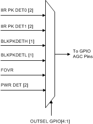 Figure 129. GPIO Output MUX Implementation
8.3.9 Power-Down Mode
The ADC31RF80 provides a lot of configurability for the power-down mode. Power-down can be enabled using the PDN pin or the SPI register writes.
8.3.10 ADC Test Pattern
The ADC31RF80 provides several different options to output test patterns instead of the actual output data of the ADC in order to simplify the serial interface and system debug of the JESD204B digital interface link. Figure 130 shows the output data path.
 Figure 130. Test Pattern Generator Implementation
8.3.10.1 Digital Block
The ADC test pattern replaces the actual output data of the ADC. The test patterns listed in Table 11 are available when the DDC is enabled and located in register 37h of the decimation filter page. When programmed, the test patterns are output for each converter (M) stream. The number of converter streams increases by 2 when complex (I, Q) output or dual-band DDC is selected.
Additionally, a 12-bit test pattern is also available.
NOTE
The number of converters increases in dual-band DDC mode and with a complex output.
Table 11. Test Pattern Options (Register 37h and 38h in Decimation Filter Page)
| BIT | NAME | DEFAULT | DESCRIPTION |
|---|---|---|---|
| Address 37h, 38h (bits 7-0) | TEST PATTERN DDC1 I-DATA, TEST PATTERN DDC1 Q-DATA, TEST PATTERN DDC2 I-DATA, TEST PATTERN DDC2 Q-DATA, |
0000 | Test pattern outputs on when the I and Q stream DDC option is chosen. 0000 = Normal operation using ADC output data 0001 = Outputs all 0s 0010 = Outputs all 1s 0011 = Outputs toggle pattern: output data are an alternating sequence of 10101010101010 and 01010101010101 0100 = Output digital ramp: output data increment by one LSB every clock cycle from code 0 to 65535 0110 = Single pattern: output data are a custom pattern 1 (75h and 76h) 0111 Double pattern: output data alternate between custom pattern 1 and custom pattern 2 1000 = Deskew pattern: output data are AAAAh 1001 = SYNC pattern: output data are FFFFh |
8.3.10.2 Transport Layer
The transport layer maps the ADC output data into 8-bit octets and constructs the JESD204B frames using the LMFS parameters. Tail bits or 0's are added when needed. Alternatively, the JESD204B long transport layer test pattern can be substituted, as shown in Table 12, instead of the ADC data with the JESD frame.
Table 12. Transport Layer Test Mode EN (Register 01h)
| BIT | NAME | DEFAULT | DESCRIPTION |
|---|---|---|---|
| 4 | TESTMODE EN | 0 | Generates long transport layer test pattern mode according to section 5.1.6.3 of the JESD204B specification. 0 = Test mode disabled 1 = Test mode disabled |
8.3.10.3 Link Layer
The link layer contains the scrambler and the 8b, 10b encoding of any data passed on from the transport layer. Additionally, the link layer also handles the initial lane alignment sequence that can be manually restarted.
The link layer test patterns are intended for testing the quality of the link (jitter testing and so forth). The test patterns do not pass through the 8b, 10b encoder and contain the options listed in Table 13.
Table 13. Link Layer Test Mode (Register 03h)
| BIT | NAME | DEFAULT | DESCRIPTION |
|---|---|---|---|
| 7-5 | LINK LAYER TESTMODE | 000 | Generates a pattern according to section 5.3.3.8.2 of the JESD204B document. 000 = Normal ADC data 001 = D21.5 (high-frequency jitter pattern) 010 = K28.5 (mixed-frequency jitter pattern) 011 = Repeat the initial lane alignment (generates a K28.5 character and repeats lane alignment sequences continuously) 100 = 12-octet random pattern (RPAT) jitter pattern |
Furthermore, a 215 pseudo-random binary sequence (PRBS) can be enabled by setting up a custom test pattern (AAAAh) in the ADC section and running AAAAh through the 8b, 10b encoder with scrambling enabled.
8.4 Device Functional Modes
8.4.1 Device Configuration
The ADC31RF80 can be configured using a serial programming interface, as described in the Serial Interface section. In addition, the device has one dedicated parallel pin (PDN) for controlling the power-down modes.
8.4.2 JESD204B Interface
The ADC31RF80 supports device subclass 1 with a maximum output data rate of 12.5 Gbps for each serial transmitter.
An external SYSREF signal is used to align all internal clock phases and the local multiframe clock to a specific sampling clock edge. This alignment allows synchronization of multiple devices in a system and minimizes timing and alignment uncertainty. Figure 131 shows that the SYNCB input is used to control the JESD204B SerDes blocks.
Depending on the ADC sampling rate, the JESD204B output interface can be operated with one, two, or four lanes. The JESD204B setup and configuration of the frame assembly parameters is controlled through the SPI interface.
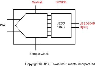 Figure 131. JESD Signal Overview
The JESD204B transmitter block, shown in Figure 132, consists of the transport layer, the data scrambler, and the link layer. The transport layer maps the ADC output data into the selected JESD204B frame data format and manages if the ADC output data or test patterns are transmitted. The link layer performs the 8b, 10b data encoding as well as the synchronization and initial lane alignment using the SYNC input signal. Optionally, data from the transport layer can be scrambled.
 Figure 132. JESD Digital Block Implementation
8.4.2.1 JESD204B Initial Lane Alignment (ILA)
The receiving device starts the initial lane alignment process by deasserting the SYNCB signal. The SYNCB signal can be issued using the SYNCB input pins or by setting the proper SPI bits. When a logic low is detected on the SYNCB input, as shown in Figure 133, the ADC31RF80 starts transmitting comma (K28.5) characters to establish the code group synchronization.
When synchronization completes, the receiving device reasserts the SYNCB signal and the ADC31RF80 starts the initial lane alignment sequence with the next local multiframe clock boundary. The ADC31RF80 transmits four multiframes, each containing K frames (K is SPI programmable). Each of the multiframes contains the frame start and end symbols. The second multiframe also contains the JESD204 link configuration data.
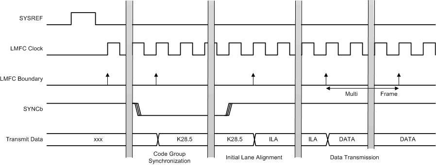 Figure 133. JESD Internal Timing Information
8.4.2.2 JESD204B Frame Assembly
The JESD204B standard defines the following parameters:
- F is the number of octets per frame clock period
- L is the number of lanes per link
- M is the number of converters for the device
- S is the number of samples per frame
8.4.2.3 JESD204B Frame Assembly with Decimation (Single-Band DDC): Complex Output
Table 14 lists the available JESD204B interface formats and valid ranges for the ADC31RF80 with decimation (single-band DDC) when using a complex output format. The ranges are limited by the SerDes line rate and the maximum ADC sample frequency. Table 15 shows the sample alignment on the different lanes.
Table 14. JESD Mode Options: Single-Band Complex Output
| DECIMATION SETTING (Complex) | NUMBER OF ACTIVE DDCS | L | M | F | S | PLL MODE | JESD MODE0 | JESD MODE1 | JESD MODE2 | RATIO [fSerDes / fCLK (Gbps / GSPS)] |
|---|---|---|---|---|---|---|---|---|---|---|
| Divide-by-4 | 1 | 4 | 2 | 1 | 1 | 20x | 1 | 1 | 0 | 2.5 |
| 4 | 2 | 2 | 2 | 20x | 1 | 0 | 0 | |||
| 2 | 2 | 2 | 1 | 40x | 0 | 0 | 1 | 5 | ||
| 2 | 2 | 4 | 2 | 40x | 2 | 0 | 0 | |||
| Divide-by-6 | 1 | 4 | 2 | 1 | 1 | 20x | 1 | 1 | 0 | 1.67 |
| 4 | 2 | 2 | 2 | 20x | 1 | 0 | 0 | |||
| 2 | 2 | 2 | 1 | 40x | 0 | 0 | 1 | 3.33 | ||
| 2 | 2 | 4 | 2 | 40x | 2 | 0 | 0 | |||
| Divide-by-8 | 1 | 2 | 2 | 2 | 1 | 20x | 1 | 0 | 0 | 2.5 |
| 1 | 2 | 4 | 1 | 40x | 2 | 0 | 0 | 5 | ||
| Divide-by-9 | 1 | 2 | 2 | 2 | 1 | 20x | 1 | 0 | 0 | 2.22 |
| 1 | 2 | 4 | 1 | 40x | 2 | 0 | 0 | 4.44 | ||
| Divide-by-10 | 1 | 2 | 2 | 2 | 1 | 20x | 1 | 0 | 0 | 2 |
| 1 | 2 | 4 | 1 | 40x | 2 | 0 | 0 | 4 | ||
| Divide-by-12 | 1 | 2 | 2 | 2 | 1 | 20x | 1 | 0 | 0 | 1.67 |
| 1 | 2 | 4 | 1 | 40x | 2 | 0 | 0 | 3.33 | ||
| Divide-by-16 | 1 | 2 | 2 | 2 | 1 | 20x | 1 | 0 | 0 | 1.25 |
| 1 | 2 | 4 | 1 | 40x | 2 | 0 | 0 | 2.5 | ||
| Divide-by-18 | 1 | 2 | 2 | 2 | 1 | 20x | 1 | 0 | 0 | 1.11 |
| 1 | 2 | 4 | 1 | 40x | 2 | 0 | 0 | 2.22 | ||
| Divide-by-20 | 1 | 2 | 2 | 2 | 1 | 20x | 1 | 0 | 0 | 1 |
| 1 | 2 | 4 | 1 | 40x | 2 | 0 | 0 | 2 | ||
| Divide-by-24 | 1 | 1 | 2 | 4 | 1 | 20x | 1 | 0 | 0 | 1.67 |
| Divide-by-32 | 1 | 1 | 2 | 4 | 1 | 40x | 2 | 0 | 0 | 1.25 |
Table 15. JESD Sample Lane Alignments: Single-Band Complex Output
| OUTPUT LANE | LMFS = 8411 | LMFS = 8422 | LMFS = 4421 20X | LMFS = 4421 40X | LMFS = 4442 | LMFS = 2441 | |||||||||
|---|---|---|---|---|---|---|---|---|---|---|---|---|---|---|---|
| D0 | AI0
[15:8] |
AI0
[15:8] |
AI0
[7:0] |
AI0
[15:8] |
AI0
[7:0] |
||||||||||
| D1 | AI0
[7:0] |
AI1
[15:8] |
AI1
[7:0] |
AQ0
[15:8] |
AQ0
[7:0] |
AI0
[15:8] |
AI0
[7:0] |
AI0
[15:8] |
AI0
[7:0] |
AI1
[15:8] |
AI1
[7:0] |
AI0
[15:8] |
AI0
[7:0] |
AQ0
[15:8] |
AQ0
[7:0] |
| D2 | AQ0
[15:8] |
AQ0
[15:8] |
AQ0
[7:0] |
AQ0
[15:8] |
AQ0
[7:0] |
AQ0
[15:8] |
AQ0
[7:0] |
AQ1
[15:8] |
AQ1
[7:0] |
||||||
| D3 | AQ0
[7:0] |
AQ1
[15:8] |
AQ1
[7:0] |
||||||||||||
8.4.2.4 JESD204B Frame Assembly with Decimation (Single-Band DDC): Real Output
Table 16 lists the available JESD204B formats and valid ranges for the ADC31RF80 with decimation (single-band DDC) when using real output format. The ranges are limited by the SerDes line rate and the maximum ADC sample frequency. Table 17 shows the sample alignment on the different lanes.
Table 16. JESD Mode Options: Single-Band Real Output (Wide Bandwidth)
| DECIMATION SETTING (Complex) | NUMBER OF ACTIVE DDCS | L | M | F | S | PLL MODE | JESD MODE0 | JESD MODE1 | JESD MODE2 | RATIO [fSerDes / fCLK (Gbps / GSPS)] |
|---|---|---|---|---|---|---|---|---|---|---|
| Divide-by-4 (Divide-by-2 real) |
1 | 4 | 1 | 2 | 4 | 20x | 1 | 0 | 0 | 2.5 |
| 2 | 1 | 4 | 4 | 40x | 2 | 0 | 0 | 5 | ||
| 2 | 1 | 1 | 1 | 40x | 0 | 0 | 1 | |||
| Divide-by-6 (Divide-by-3 real) |
1 | 4 | 1 | 2 | 4 | 20x | 1 | 0 | 0 | 1.67 |
| 2 | 1 | 4 | 4 | 40x | 2 | 0 | 0 | 3.33 | ||
| 2 | 1 | 1 | 1 | 40x | 0 | 0 | 1 |
Table 17. JESD Sample Lane Alignment: Single-Band Real Output (Wide Bandwidth)
| OUTPUT LANE | LMFS = 8224 | LMFS = 4244 | LMFS = 4211 | ||||
|---|---|---|---|---|---|---|---|
| D0 | A0[15:8] | A0[7:0] | |||||
| D1 | A1[15:8] | A1[7:0] | A0[15:8] | A0[7:0] | A1[15:8] | A1[7:0] | A0[15:8] |
| D2 | A2[15:8] | A2[7:0] | A2[15:8] | A2[7:0] | A3[15:8] | A3[7:0] | A0[7:0] |
| D3 | A3[15:8] | A3[7:0] | |||||
8.4.2.5 JESD204B Frame Assembly with Decimation (Single-Band DDC): Real Output
Table 18 lists the available JESD204B formats and valid ranges for the ADC31RF80 with decimation (dual-band DDC) when using a complex output format. Table 19 shows the sample alignment on the different lanes.
Table 18. JESD Mode Options: Single-Band Real Output
| DECIMATION SETTING (Complex) | NUMBER OF ACTIVE DDCS | L | M | F | S | PLL MODE | JESD MODE0 | JESD MODE1 | JESD MODE2 | RATIO [fSerDes / fCLK (Gbps / GSPS)] |
|---|---|---|---|---|---|---|---|---|---|---|
| Divide-by-8 (Divide-by-4 real) |
1 | 2 | 1 | 1 | 1 | 20x | 1 | 1 | 0 | 2.5 |
| 2 | 1 | 2 | 2 | 20x | 1 | 0 | 0 | |||
| 1 | 1 | 2 | 1 | 40x | 0 | 0 | 1 | 5 | ||
| 1 | 1 | 4 | 2 | 40x | 2 | 0 | 0 | |||
| Divide-by-9 (Divide-by-4.5 real) |
1 | 2 | 1 | 1 | 1 | 20x | 1 | 1 | 0 | 2.22 |
| 2 | 1 | 2 | 2 | 20x | 1 | 0 | 0 | |||
| 1 | 1 | 2 | 1 | 40x | 0 | 0 | 1 | 4.44 | ||
| 1 | 1 | 4 | 2 | 40x | 2 | 0 | 0 | |||
| Divide-by-10 (Divide-by-5 real) |
1 | 2 | 1 | 1 | 1 | 20x | 1 | 1 | 0 | 2 |
| 2 | 1 | 2 | 2 | 20x | 1 | 0 | 0 | |||
| 1 | 1 | 2 | 1 | 40x | 0 | 0 | 1 | 4 | ||
| 1 | 1 | 4 | 2 | 40x | 2 | 0 | 0 | |||
| Divide-by-12 (Divide-by-6 real) |
1 | 2 | 1 | 1 | 1 | 20x | 1 | 1 | 0 | 1.67 |
| 2 | 1 | 2 | 2 | 20x | 1 | 0 | 0 | |||
| 1 | 1 | 2 | 1 | 40x | 0 | 0 | 1 | 3.33 | ||
| 1 | 1 | 4 | 2 | 40x | 2 | 0 | 0 | |||
| Divide-by-16 (Divide-by-8 real) |
1 | 2 | 1 | 1 | 1 | 20x | 1 | 1 | 0 | 1.25 |
| 2 | 1 | 2 | 2 | 20x | 1 | 0 | 0 | |||
| 1 | 1 | 2 | 1 | 40x | 0 | 0 | 1 | 2.5 | ||
| 1 | 1 | 4 | 2 | 40x | 2 | 0 | 0 | |||
| Divide-by-18 (Divide-by-9 real) |
1 | 2 | 1 | 1 | 1 | 20x | 1 | 1 | 0 | 1.11 |
| 2 | 1 | 2 | 2 | 20x | 1 | 0 | 0 | |||
| 1 | 1 | 2 | 1 | 40x | 0 | 0 | 1 | 2.22 | ||
| 1 | 1 | 4 | 2 | 40x | 2 | 0 | 0 | |||
| Divide-by-20 (Divide-by-10 real) |
1 | 2 | 1 | 1 | 1 | 20x | 1 | 1 | 0 | 1 |
| 2 | 1 | 2 | 2 | 20x | 1 | 0 | 0 | |||
| 1 | 1 | 2 | 1 | 40x | 0 | 0 | 1 | 2 | ||
| 1 | 1 | 4 | 2 | 40x | 2 | 0 | 0 | |||
| Divide-by-24 (Divide-by-12 real) |
1 | 1 | 1 | 2 | 1 | 40x | 0 | 0 | 1 | 1.67 |
| 1 | 1 | 4 | 2 | 40x | 2 | 0 | 0 | |||
| Divide-by-32 (Divide-by-16 real) |
1 | 1 | 1 | 2 | 1 | 40x | 0 | 0 | 1 | 1.25 |
| 1 | 1 | 4 | 2 | 40x | 2 | 0 | 0 |
Table 19. JESD Sample Lane Assignment: Single-Band Real Output
| OUTPUT LANE | LMFS = 4211 | LMFS = 4222 | LMFS = 2221 | LMFS = 2242 | |||||
|---|---|---|---|---|---|---|---|---|---|
| D0 | A0[15:8] | A0[15:8] | A0[7:0] | ||||||
| D1 | A0[7:0] | A1[15:8] | A1[7:0] | A0 [15:8] | A0[7:0] | A0[15:8] | A0[7:0] | A1[15:8] | A1[7:0] |
8.4.2.6 JESD204B Frame Assembly with Decimation (Dual-Band DDC): Complex Output
Table 20 lists the available JESD204B formats and valid ranges for the ADC31RF80 with decimation (dual-band DDC) when using a complex output format. The ranges are limited by the SerDes line rate and the maximum ADC sample frequency. Table 21 shows the sample alignment on the different lanes.
Table 20. JESD Mode Options: Dual-Band Complex Output
| DECIMATION SETTING (Complex) | NUMBER OF ACTIVE DDCS | L | M | F | S | PLL MODE | JESD MODE0 | JESD MODE1 | JESD MODE2 | RATIO [fSerDes / fCLK (Gbps / GSPS)] |
|---|---|---|---|---|---|---|---|---|---|---|
| Divide-by-8 | 2 | 4 | 4 | 2 | 1 | 20x | 1 | 0 | 0 | 2.5 |
| 2 | 4 | 4 | 1 | 40x | 2 | 0 | 0 | 5 | ||
| Divide-by-9 | 2 | 4 | 4 | 2 | 1 | 20x | 1 | 0 | 0 | 2.22 |
| 2 | 4 | 4 | 1 | 40x | 2 | 0 | 0 | 4.44 | ||
| Divide-by-10 | 2 | 4 | 4 | 2 | 1 | 20x | 1 | 0 | 0 | 2 |
| 2 | 4 | 4 | 1 | 40x | 2 | 0 | 0 | 4 | ||
| Divide-by-12 | 2 | 4 | 4 | 2 | 1 | 20x | 1 | 0 | 0 | 1.67 |
| 2 | 4 | 4 | 1 | 40x | 2 | 0 | 0 | 3.33 | ||
| Divide-by-16 | 2 | 4 | 4 | 2 | 1 | 20x | 1 | 0 | 0 | 1.25 |
| 2 | 4 | 4 | 1 | 40x | 2 | 0 | 0 | 2.5 | ||
| Divide-by-18 | 2 | 4 | 4 | 2 | 1 | 20x | 1 | 0 | 0 | 1.11 |
| 2 | 4 | 4 | 1 | 40x | 2 | 0 | 0 | 2.22 | ||
| Divide-by-20 | 2 | 4 | 4 | 2 | 1 | 20x | 1 | 0 | 0 | 1 |
| 2 | 4 | 4 | 1 | 40x | 2 | 0 | 0 | 2 | ||
| Divide-by-24 | 2 | 2 | 4 | 4 | 1 | 40x | 2 | 0 | 0 | 1.67 |
| Divide-by-32 | 2 | 2 | 4 | 4 | 1 | 40x | 2 | 0 | 0 | 1.25 |
Table 21. JESD Sample Lane Assignment: Dual-Band Complex Output(1)
| OUTPUT LANE | LMFS = 8821 | LMFS = 4841 | ||||
|---|---|---|---|---|---|---|
| D0 | A10[15:8] | A10[7:0] | ||||
| D1 | A1Q0[15:8] | A1Q0[7:0] | A1I0[15:8] | A1I0[7:0] | A1Q0[15:8] | A1Q0[7:0] |
| D2 | A2I0[15:8] | A2I0[7:0] | A2I0[15:8] | A2I0[7:0] | A2Q0[15:8] | A2Q0[7:0] |
| D3 | A2Q0[15:8] | A2Q0[7:0] | ||||
8.4.2.7 JESD204B Frame Assembly with Decimation (Dual-Band DDC): Real Output
Table 22 lists the available JESD204B formats and valid ranges for the ADC31RF80 with decimation (dual-band DDC) when using real output format. The ranges are limited by the SerDes line rate and the maximum ADC sample frequency. Table 23 shows the sample alignment on the different lanes.
Table 22. JESD Mode Options: Dual-Band Real Output
| DECIMATION SETTING (Complex) | NUMBER OF ACTIVE DDCS | L | M | F | S | PLL MODE | JESD MODE0 | JESD MODE1 | JESD MODE2 | RATIO [fSerDes / fCLK (Gbps / GSPS)] |
|---|---|---|---|---|---|---|---|---|---|---|
| Divide-by-8 (Divide-by-4 real) |
2 | 4 | 2 | 1 | 1 | 20x | 1 | 1 | 0 | 2.5 |
| 4 | 2 | 2 | 2 | 20x | 1 | 0 | 0 | |||
| 2 | 2 | 2 | 1 | 40x | 0 | 0 | 1 | 5 | ||
| 2 | 2 | 4 | 2 | 40x | 2 | 0 | 0 | |||
| Divide-by-9 (Divide-by-4.5 real) |
2 | 4 | 2 | 1 | 1 | 20x | 1 | 1 | 0 | 2.22 |
| 4 | 2 | 2 | 2 | 20x | 1 | 0 | 0 | |||
| 2 | 2 | 2 | 1 | 40x | 0 | 0 | 1 | 4.44 | ||
| 2 | 2 | 4 | 2 | 40x | 2 | 0 | 0 | |||
| Divide-by-10 (Divide-by-5 real) |
2 | 4 | 2 | 1 | 1 | 20x | 1 | 1 | 0 | 2 |
| 4 | 2 | 2 | 2 | 20x | 1 | 0 | 0 | |||
| 2 | 2 | 2 | 1 | 40x | 0 | 0 | 1 | 4 | ||
| 2 | 2 | 4 | 2 | 40x | 2 | 0 | 0 | |||
| Divide-by-12 (Divide-by-6 real) |
2 | 4 | 2 | 1 | 1 | 20x | 1 | 1 | 0 | 1.67 |
| 4 | 2 | 2 | 2 | 20x | 1 | 0 | 0 | |||
| 2 | 2 | 2 | 1 | 40x | 0 | 0 | 1 | 3.33 | ||
| 2 | 2 | 4 | 2 | 40x | 2 | 0 | 0 | |||
| Divide-by-16 (Divide-by-8 real) |
2 | 4 | 2 | 1 | 1 | 20x | 1 | 1 | 0 | 1.25 |
| 4 | 2 | 2 | 2 | 20x | 1 | 0 | 0 | |||
| 2 | 2 | 2 | 1 | 40x | 0 | 0 | 1 | 2.5 | ||
| 2 | 2 | 4 | 2 | 40x | 2 | 0 | 0 | |||
| Divide-by-18 (Divide-by-9 real) |
2 | 4 | 2 | 1 | 1 | 20x | 1 | 1 | 0 | 1.11 |
| 4 | 2 | 2 | 2 | 20x | 1 | 0 | 0 | |||
| 2 | 2 | 2 | 1 | 40x | 0 | 0 | 1 | 2.22 | ||
| 2 | 2 | 4 | 2 | 40x | 2 | 0 | 0 | |||
| Divide-by-20 (Divide-by-10 real) |
2 | 4 | 2 | 1 | 1 | 20x | 1 | 1 | 0 | 1 |
| 4 | 2 | 2 | 2 | 20x | 1 | 0 | 0 | |||
| 2 | 2 | 2 | 1 | 40x | 0 | 0 | 1 | 2 | ||
| 2 | 2 | 4 | 2 | 40x | 2 | 0 | 0 | |||
| Divide-by-24 (Divide-by-12 real) |
2 | 2 | 2 | 2 | 1 | 40x | 0 | 0 | 1 | 1.67 |
| 2 | 2 | 4 | 2 | 40x | 2 | 0 | 0 | |||
| Divide-by-32 (Divide-by-16 real) |
2 | 2 | 2 | 2 | 1 | 40x | 0 | 0 | 1 | 1.25 |
| 2 | 2 | 4 | 2 | 40x | 2 | 0 | 0 |
Table 23. JESD Sample Lane Assignment: Dual-Band Complex Output(1)
| OUTPUT LANE | LMFS = 8411 | LMFS = 8422 | LMFS = 4421 | LMFS = 4442 | |||||
|---|---|---|---|---|---|---|---|---|---|
| D0 | A10[15:8] | A10[15:8] | A10[7:0] | ||||||
| D1 | A10[7:0] | A11[15:8] | A11[7:0] | A10[15:8] | A10[7:0] | A10[15:8] | A10[7:0] | A11[15:8] | A11[7:0] |
| D2 | A20[15:8] | A20[15:8] | A20[7:0] | A20[15:8] | A20[7:0] | A20[15:8] | A20[7:0] | A21[15:8] | A21[7:0] |
| D3 | A20[7:0] | A21[15:8] | A21[7:0] | ||||||
8.4.3 Serial Interface
The ADC has a set of internal registers that can be accessed by the serial interface formed by the SEN (serial interface enable), SCLK (serial interface clock), and SDIN (serial interface data) pins. Serially shifting bits into the device is enabled when SEN is low. Figure 134 shows that SDIN serial data are latched at every SCLK rising edge when SEN is active (low). Table 24 also shows that the interface can function with SCLK frequencies from 20 MHz down to low speeds (of a few hertz) and also with a non-50% SCLK duty cycle.
The SPI access uses 24 bits consisting of eight register data bits, 12 register address bits, and four special bits to distinguish between read/write, page and register, and individual channel access, as described in Table 25.
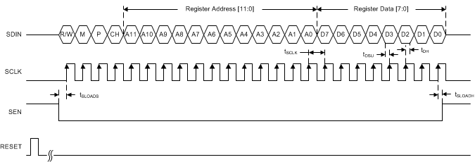 Figure 134. SPI Timing Diagram
Table 24. SPI Timing Information
| MIN | TYP | MAX | UNIT | ||
|---|---|---|---|---|---|
| fSCLK | SCLK frequency (equal to 1 / tSCLK) | 1 | 20 | MHz | |
| tSLOADS | SEN to SCLK setup time | 50 | ns | ||
| tSLOADH | SCLK to SEN hold time | 50 | ns | ||
| tDSU | SDIN setup time | 10 | ns | ||
| tDH | SDIN hold time | 10 | ns | ||
| tSDOUT | Delay between SCLK falling edge to SDOUT | 10 | ns | ||
Table 25. SPI Input Description
| SPI BIT | DESCRIPTION | OPTIONS |
|---|---|---|
| R/W bit | Read/write bit | 0 = SPI write 1 = SPI read back |
| M bit | SPI bank access | 0 = Analog SPI bank (master) 1 = All digital SPI banks (main digital, interleaving, decimation filter, JESD digital, and so forth) |
| P bit | JESD page selection bit | 0 = Page access 1 = Register access |
| CH bit | SPI access for a specific channel of the JESD SPI bank. Useful for the dual-channel device, ADC32RF80. | — |
| ADDR[11:0] | SPI address bits | — |
| DATA[7:0] | SPI data bits | — |
Figure 135 shows the SDOUT timing when data are read back from a register. Data are placed on the SDOUT bus at the SCLK falling edge after a delay of tSDOUT (10 ns typical) so that the data can be latched at the SCLK rising edge by the external receiver.
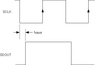 Figure 135. SDOUT Timing
8.4.3.1 Serial Register Write: Analog Bank
The internal register of the ADC31RF80 analog bank (Figure 136) can be programmed by:
- Driving the SEN pin low.
- Initiating a serial interface cycle selecting the page address of the register whose content must be written. To select the master page: write address 0012h with 04h. To select the ADC page: write address 0011h with FFh.
- Writing the register content. When a page is selected, multiple registers located in the same page can be programmed.
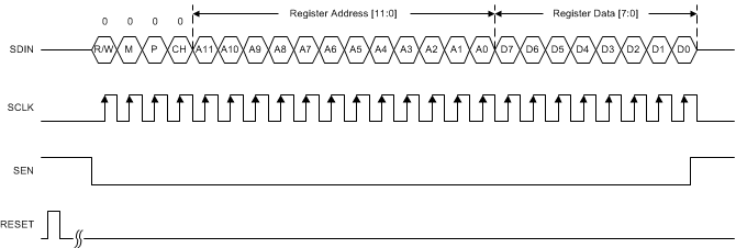 Figure 136. SPI Write Timing Diagram for the Analog Bank
8.4.3.2 Serial Register Readout: Analog Bank
Contents of the registers located in the two pages of the analog bank (Figure 137) can be readback by:
- Driving the SEN pin low.
- Selecting the page address of the register whose content must be read. Master page: write address 0012h with 04h. ADC page: write address 0011h with FFh.
- Setting the R/W bit to 1 and writing the address to be read back.
- Reading back the register content on the SDOUT pin. When a page is selected, the contents of multiple registers located in same page can be readback.
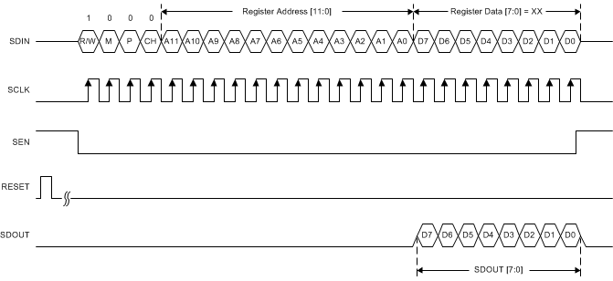 Figure 137. SPI Read Timing Diagram for the Analog Bank
8.4.3.3 Serial Register Write: Digital Bank
The digital bank contains four pages (the offset corrector page, digital gain page, main digital page, and JESD digital page). Figure 138 shows the timing for the individual page selection. The registers located in the pages of the digital bank can be programmed by:
- Driving the SEN pin low.
- Setting the M bit to 1 and specifying the page with with the desired register. There are seven pages in Digital Bank. These pages can be selected by appropriately programming register bits DIGITAL BANK PAGE SEL, located in addresses 002h, 003h, and 004h, using three consecutive SPI cycles. Addressing in a SPI cycle begins with 4xxx when selecting a page from digital bank because the M bit must be set to 1.
- To select the offset corrector page: write address 4004h with 61h, 4003h with 00h, and 4002h with 00h.
- To select the digital gain page: write address 4004h with 61h, 4003h with 00h, and 4002h with 05h.
- To select the main digital page: write address 4004h with 68h, 4003h with 00h, and 4002h with 00h.
- To select the JESD digital page: write address 4004h with 69h, 4003h with 00h, and 4002h with 00h.
- Writing into the desired register by setting both the M bit and P bit to 1. Write register content. When a page is selected, multiple writes into the same page can be done. As shown in Figure 139, addressing in an SPI cycle begins with 6xxx when selecting a page from the digital bank because the M bit must be set to 1.
 Figure 138. SPI Write Timing Diagram for Digital Bank Page Selection
Keep CH = 1 while programing registers in JESD digital page. Thus, an SPI cycle to program registers in JESD digital page begins with 7xxx.
 Figure 139. SPI Write Timing Diagram for Digital Bank Register Write
8.4.3.4 Serial Register Readout: Digital Bank
Readback of the register in one of the digital banks (as shown in Figure 140) can be accomplished by:
- Driving the SEN pin low.
- Selecting the page in the digital page: follow step 2 in the Serial Register Write: Digital Bank section.
- Set the R/W, M, P, and CH bits to 1, and write the address to be read back.
- Read back the register content on the SDOUT pin. When a page is selected, multiple read backs from the same page can be done.
 Figure 140. SPI Read Timing Diagram for the Digital Bank
8.4.3.5 Serial Register Write: Decimation Filter and Power Detector Pages
The decimation filter and power detector pages are special pages that accept direct addressing. The sampling clock and SYSREF signal are required to properly configure the decimation settings. Registers located in these pages can be programmed in one SPI cycle (Figure 141).
- Drive the SEN pin low.
- Directly write to the decimation filter or power detector pages. To program registers in these pages, set M = 1 and CH = 1. Additionally, address bit A[10] selects the decimation filter page (A[10] = 0) or the power detector page (A[10] = 1).
- Decimation filter page: SPI cycle begins with 50xxh.
- Power detector page: SPI cycle begins with 54xxh.
 Figure 141. SPI Write Timing Diagram for the Decimation and Power Detector Pages
8.5 Register Maps
The ADC31RF80 contains two main SPI banks. The analog SPI bank provides access to the ADC core and the digital SPI bank controls the digital blocks (including the serial JESD interface). Figure 142 and Figure 143 provide a conceptual view of the SPI registers inside the ADC31RF80. The analog SPI bank contains the master and ADC pages. The digital SPI bank is divided into multiple pages (the main digital, digital gain, decimation filter, JESD digital, and power detector pages).
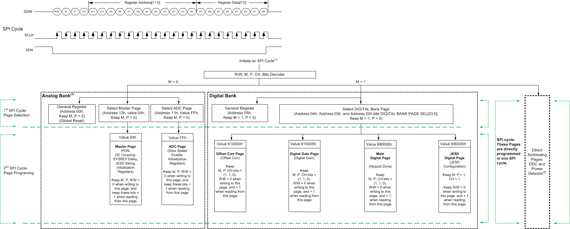
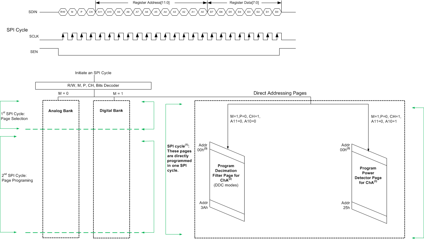
Table 26 lists the register map for the ADC31RF80.
Table 26. Register Map
| REGISTER ADDRESS A[11:0] (Hex) |
REGISTER DATA | |||||||
|---|---|---|---|---|---|---|---|---|
| 7 | 6 | 5 | 4 | 3 | 2 | 1 | 0 | |
| GENERAL REGISTERS | ||||||||
| 000 | RESET | 0 | 0 | 0 | 0 | 0 | 0 | RESET |
| 002 | DIGITAL BANK PAGE SEL[7:0] | |||||||
| 003 | DIGITAL BANK PAGE SEL[15:8] | |||||||
| 004 | DIGITAL BANK PAGE SEL[23:16] | |||||||
| 010 | 0 | 0 | 0 | 0 | 0 | 0 | 0 | 3 or 4 WIRE |
| 011 | ADC PAGE SEL | |||||||
| 012 | 0 | 0 | 0 | 0 | 0 | MASTER PAGE SEL | 0 | 0 |
| MASTER PAGE (M = 0) | ||||||||
| 020 | 0 | 0 | 0 | PDN SYSREF | 0 | 0 | 0 | GLOBAL PDN |
| 032 | 0 | 0 | INCR CM IMPEDANCE | 0 | 0 | 0 | 0 | 0 |
| 039 | 0 | ALWAYS WRITE 1 | 0 | ALWAYS WRITE 1 | 0 | 0 | 0 | SYNC TERM DIS |
| 03C | 0 | SYSREF DEL EN | 0 | 0 | 0 | 0 | SYSREF DEL[4:3] | |
| 03D | 0 | 0 | 0 | 0 | 0 | JESD OUTPUT SWING | ||
| 05A | SYSREF DEL[2:0] | 0 | 0 | 0 | 0 | 0 | ||
| 057 | 0 | 0 | 0 | SEL SYSREF REG | ASSERT SYSREF REG | 0 | 0 | 0 |
| 058 | 0 | 0 | SYNCB POL | 0 | 0 | 0 | 0 | 0 |
| ADC PAGE (FFh, M = 0) | ||||||||
| 03F | 0 | 0 | 0 | 0 | 0 | SLOW SP EN1 | 0 | 0 |
| 042 | 0 | 0 | 0 | SLOW SP EN2 | 0 | 0 | 1 | 1 |
| Offset Corr Page (610000h, M = 1) | ||||||||
| 68 | FREEZE OFFSET CORR | ALWAYS WRITE 1 | 0 | 0 | 0 | DIS OFFSET CORR | ALWAYS WRITE 1 | 0 |
| Digital Gain Page (610005, M = 1) | ||||||||
| 0A6 | 0 | 0 | 0 | 0 | DIGITAL GAIN | |||
| Main Digital Page (680000h, M = 1) | ||||||||
| 000 | 0 | 0 | 0 | 0 | 0 | 0 | 0 | DIG CORE RESET GBL |
| 0A2 | 0 | 0 | 0 | 0 | NQ ZONE EN | NYQUIST ZONE | ||
| 0A5 | Sampling Frequency | |||||||
| 0A9 | 0 | 0 | 0 | 0 | Sampling Frequency Enable | 0 | 1 | 1 |
| 0B0 | Band1 Lower-Edge Frequency LSB Setting | |||||||
| 0B1 | 0 | 0 | 0 | Band1 Lower-Edge Frequency MSB Setting | ||||
| 0B2 | Band1 Upper-Edge Frequency LSB Setting | |||||||
| 0B3 | 0 | 0 | Band1 Frequency Range Enable | Band1 Upper-Edge Frequency MSB Setting | ||||
| 0B4 | Band2 Lower-Edge Frequency LSB Setting | |||||||
| 0B5 | 0 | 0 | 0 | Band2 Lower-Edge Frequency MSB Setting | ||||
| 0B6 | Band2 Upper-Edge Frequency LSB Setting | |||||||
| 0B7 | 0 | 0 | Band2 Frequency Range Enable | Band2 Upper-Edge Frequency MSB Setting | ||||
| 0B8 | Band3 Lower-Edge Frequency LSB Setting | |||||||
| 0B9 | 0 | 0 | 0 | Band3 Lower-Edge Frequency MSB Setting | ||||
| 0BA | Band3 Upper-Edge Frequency LSB Setting | |||||||
| 0BB | 0 | 0 | Band3 Frequency Range Enable | Band3 Upper-Edge Frequency MSB Setting | ||||
| JESD DIGITAL PAGE (690000h, M = 1) | ||||||||
| 001 | CTRL K | 0 | 0 | TESTMODE EN | 0 | LANE ALIGN | FRAME ALIGN | TX LINK DIS |
| 002 | SYNC REG | SYNC REG EN | 0 | 0 | 12BIT MODE | JESD MODE0 | ||
| 003 | LINK LAYER TESTMODE | LINK LAY RPAT | LMFC MASK RESET | JESD MODE1 | JESD MODE2 | RAMP 12BIT | ||
| 004 | 0 | 0 | 0 | 0 | 0 | 0 | REL ILA SEQ | |
| 006 | SCRAMBLE EN | 0 | 0 | 0 | 0 | 0 | 0 | 0 |
| 007 | 0 | 0 | 0 | FRAMES PER MULTIFRAME (K) | ||||
| 016 | 0 | 40X MODE | 0 | 0 | 0 | 0 | ||
| 017 | 0 | 0 | 0 | 0 | LANE0 POL |
LANE1 POL |
LANE2 POL |
LANE3 POL |
| 032 | SEL EMP LANE 0 | 0 | 0 | |||||
| 033 | SEL EMP LANE 1 | 0 | 0 | |||||
| 034 | SEL EMP LANE 2 | 0 | 0 | |||||
| 035 | SEL EMP LANE 3 | 0 | 0 | |||||
| 036 | 0 | CMOS SYNCB | 0 | 0 | 0 | 0 | 0 | 0 |
| 037 | 0 | 0 | 0 | 0 | 0 | 0 | PLL MODE | |
| 03C | 0 | 0 | 0 | 0 | 0 | 0 | 0 | EN CMOS SYNCB |
| 03E | 0 | MASK CLKDIV SYSREF | MASK NCO SYSREF | 0 | 0 | 0 | 0 | 0 |
| DECIMATION FILTER PAGE (Direct Addressing, 16-Bit Address, 5000h) | ||||||||
| 000 | 0 | 0 | 0 | 0 | 0 | 0 | 0 | DDC EN |
| 001 | 0 | 0 | 0 | 0 | DECIM FACTOR | |||
| 002 | 0 | 0 | 0 | 0 | 0 | 0 | 0 | DUAL BAND EN |
| 005 | 0 | 0 | 0 | 0 | 0 | 0 | 0 | REAL OUT EN |
| 007 | DDC0 NCO1 LSB | |||||||
| 008 | DDC0 NCO1 MSB | |||||||
| 009 | DDC0 NCO2 LSB | |||||||
| 00A | DDC0 NCO2 MSB | |||||||
| 00B | DDC0 NCO3 LSB | |||||||
| 00C | DDC0 NCO3 MSB | |||||||
| 00D | DDC1 NCO4 LSB | |||||||
| 00E | DDC1 NCO4 MSB | |||||||
| 00F | 0 | 0 | 0 | 0 | 0 | 0 | 0 | NCO SEL PIN |
| 010 | 0 | 0 | 0 | 0 | 0 | 0 | NCO SEL | |
| 011 | 0 | 0 | 0 | 0 | 0 | 0 | LMFC RESET MODE | |
| 014 | 0 | 0 | 0 | 0 | 0 | 0 | 0 | DDC0 6DB GAIN |
| 016 | 0 | 0 | 0 | 0 | 0 | 0 | 0 | DDC1 6DB GAIN |
| 01E | 0 | DDC DET LAT | 0 | 0 | 0 | 0 | ||
| 01F | 0 | 0 | 0 | 0 | 0 | 0 | 0 | WBF 6DB GAIN |
| 033 | CUSTOM PATTERN1[7:0] | |||||||
| 034 | CUSTOM PATTERN1[15:8] | |||||||
| 035 | CUSTOM PATTERN2[7:0] | |||||||
| 036 | CUSTOM PATTERN2[15:8] | |||||||
| 037 | TEST PATTERN DDC1 Q-DATA | TEST PATTERN DDC1 I-DATA | ||||||
| 038 | TEST PATTERN DDC2 Q-DATA | TEST PATTERN DDC2 I -DATA | ||||||
| 039 | 0 | 0 | 0 | 0 | 0 | 0 | 0 | USE COMMON TEST PATTERN |
| 03A | 0 | 0 | 0 | 0 | 0 | 0 | TEST PAT RES | TP RES EN |
| POWER DETECTOR PAGE (Direct Addressing, 16-Bit Address, 5400h) | ||||||||
| 000 | 0 | 0 | 0 | 0 | 0 | 0 | 0 | PKDET EN |
| 001 | BLKPKDET [7:0] | |||||||
| 002 | BLKPKDET [15:8] | |||||||
| 003 | 0 | 0 | 0 | 0 | 0 | 0 | 0 | BLKPKDET [16] |
| 007 | BLKTHHH | |||||||
| 008 | BLKTHHL | |||||||
| 009 | BLKTHLH | |||||||
| 00A | BLKTHLL | |||||||
| 00B | DWELL[7:0] | |||||||
| 00C | DWELL[15:8] | |||||||
| 00D | 0 | 0 | 0 | 0 | 0 | 0 | 0 | FILT0LPSEL |
| 00E | 0 | 0 | 0 | 0 | TIMECONST | |||
| 00F | FIL0THH[7:0] | |||||||
| 010 | FIL0THH[15:8] | |||||||
| 011 | FIL0THL[7:0] | |||||||
| 012 | FIL0THL[15:8] | |||||||
| 013 | 0 | 0 | 0 | 0 | 0 | 0 | 0 | IIR0 2BIT EN |
| 016 | FIL1THH[7:0] | |||||||
| 017 | FIL1THH[15:8] | |||||||
| 018 | FIL1THL[7:0] | |||||||
| 019 | FIL1THL[15:8] | |||||||
| 01A | 0 | 0 | 0 | 0 | 0 | 0 | 0 | IIR1 2BIT EN |
| 01D | DWELLIIR[7:0] | |||||||
| 01E | DWELLIIR[15:8] | |||||||
| 020 | 0 | 0 | 0 | 0 | 0 | 0 | 0 | IIR0 2BIT EN |
| 021 | 0 | 0 | 0 | PWRDETACCU | ||||
| 022 | PWRDETH[7:0] | |||||||
| 023 | PWRDETH[15:8] | |||||||
| 024 | PWRDETL[7:0] | |||||||
| 025 | PWRDETL[15:8] | |||||||
| 027 | 0 | 0 | 0 | 0 | 0 | 0 | 0 | RMS 2BIT EN |
| 02B | 0 | 0 | 0 | RESET AGC | 0 | 0 | 0 | 0 |
| 032 | OUTSEL GPIO4 | |||||||
| 033 | OUTSEL GPIO1 | |||||||
| 034 | OUTSEL GPIO3 | |||||||
| 035 | OUTSEL GPIO2 | |||||||
| 037 | 0 | 0 | 0 | 0 | IODIR GPIO2 | IODIR GPIO3 | IODIR GPIO1 | IODIR GPIO4 |
| 038 | 0 | 0 | INSEL1 | 0 | 0 | INSEL0 | ||
8.5.1 Example Register Writes
This section provides three different example register writes. Table 27 describes a global power-down register write, Table 28 describes the register writes when the scrambler is enabled, and Table 29 describes the register writes for 8x decimation (complex output, 1 DDC mode) with the NCO set to 1.8 GHz (fS = 3 GSPS) and the JESD format configured to LMFS = 4421.
Table 27. Global Power-Down
| ADDRESS | DATA | COMMENT |
|---|---|---|
| 12h | 04h | Set the master page |
| 20h | 01h | Set the global power-down |
Table 28. Scrambler Enable
| ADDRESS | DATA | COMMENT |
|---|---|---|
| 4004h | 69h | Select the digital JESD page |
| 4003h | 00h | |
| 6006h | 80h | Scrambler enable |
Table 29. 8x Decimation
| ADDRESS | DATA | COMMENT |
|---|---|---|
| 4004h | 68h | Select the main digital page |
| 4003h | 00h | |
| 6000h | 01h | Issue a digital reset |
| 6000h | 00h | Clear the digital reset |
| 4004h | 69h | Select the digital JESD page |
| 4003h | 00h | |
| 6002h | 01h | Set JESD MODE0 = 1 |
| 5000h | 01h | Enable the DDC |
| 5001h | 02h | Set decimation to 8x complex |
| 5007h | 9Ah | Set the LSB of DDC0, NCO1 to 9Ah (fNCO = 1.8 GHz, fS = 3 GSPS) |
| 5008h | 99h | Set the MSB of DDC0, NCO1 to 99h (fNCO = 1.8 GHz, fS = 3 GSPS) |
| 5014h | 01h | Enable the 6-dB digital gain of DDC0 |
8.5.2 Register Descriptions
Table 30 lists the access codes for the ADC31RF80 registers.
Table 30. ADC31RF80 Access Type Codes
| Access Type | Code | Description |
|---|---|---|
| R | R | Read |
| R-W | R/W | Read or Write |
| W | W | Write |
| -n | Value after reset or the default value |
8.5.2.1 General Registers
8.5.2.1.1 Register 000h (address = 000h), General Registers
| 7 | 6 | 5 | 4 | 3 | 2 | 1 | 0 |
| RESET | 0 | 0 | 0 | 0 | 0 | 0 | RESET |
| R/W-0h | W-0h | W-0h | W-0h | W-0h | W-0h | W-0h | R/W-0h |
Table 31. Register 000h Field Descriptions
| Bit | Field | Type | Reset | Description |
|---|---|---|---|---|
| 7 | RESET | R/W | 0h |
0 = Normal operation 1 = Internal software reset, clears back to 0 |
| 6-1 | 0 | W | 0h | Must write 0 |
| 0 | RESET | R/W | 0h |
0 = Normal operation(1) 1 = Internal software reset, clears back to 0 |
8.5.2.1.2 Register 002h (address = 002h), General Registers
| 7 | 6 | 5 | 4 | 3 | 2 | 1 | 0 |
| DIGITAL BANK PAGE SEL[7:0] | |||||||
| R/W-0h | |||||||
Table 32. Register 002h Field Descriptions
| Bit | Field | Type | Reset | Description |
|---|---|---|---|---|
| 7-0 | DIGITAL BANK PAGE SEL[7:0] | R/W | 0h | Program the JESD BANK PAGE SEL[23:0] bits to access the desired page in the JESD bank. 680000h = Main digital page 610000h = Digital function page 690000h = JESD digital page selected |
8.5.2.1.3 Register 003h (address = 003h), General Registers
| 7 | 6 | 5 | 4 | 3 | 2 | 1 | 0 |
| DIGITAL BANK PAGE SEL[15:8] | |||||||
| R/W-0h | |||||||
Table 33. Register 003h Field Descriptions
| Bit | Field | Type | Reset | Description |
|---|---|---|---|---|
| 7-0 | DIGITAL BANK PAGE SEL[15:8] | R/W | 0h | Program the JESD BANK PAGE SEL[23:0] bits to access the desired page in the JESD bank. 680000h = Main digital page 610000h = Digital function page 690000h = JESD digital page selected |
8.5.2.1.4 Register 004h (address = 004h), General Registers
| 7 | 6 | 5 | 4 | 3 | 2 | 1 | 0 |
| DIGITAL BANK PAGE SEL[23:16] | |||||||
| R/W-0h | |||||||
Table 34. Register 004h Field Descriptions
| Bit | Field | Type | Reset | Description |
|---|---|---|---|---|
| 7-0 | DIGITAL BANK PAGE SEL[23:16] | R/W | 0h | Program the JESD BANK PAGE SEL[23:0] bits to access the desired page in the JESD bank. 680000h = Main digital page 610000h = Digital function page 690000h = JESD digital page selected |
8.5.2.1.5 Register 010h (address = 010h), General Registers
| 7 | 6 | 5 | 4 | 3 | 2 | 1 | 0 |
| 0 | 0 | 0 | 0 | 0 | 0 | 0 | 3 or 4 WIRE |
| W-0h | W-0h | W-0h | W-0h | W-0h | W-0h | W-0h | R/W-0h |
Table 35. Register 010h Field Descriptions
| Bit | Field | Type | Reset | Description |
|---|---|---|---|---|
| 7-1 | 0 | W | 0h | Must write 0 |
| 0 | 3 or 4 WIRE | R/W | 0h | 0 = 4-wire SPI (default) 1 = 3-wire SPI where SDIN become input or output |
8.5.2.1.6 Register 011h (address = 011h), General Registers
| 7 | 6 | 5 | 4 | 3 | 2 | 1 | 0 |
| ADC PAGE SEL | |||||||
| R/W-0h | |||||||
Table 36. Register 011h Field Descriptions
| Bit | Field | Type | Reset | Description |
|---|---|---|---|---|
| 7-0 | ADC PAGE SEL | R/W | 0h |
00000000 = Normal operation, ADC page is not selected 11111111 = ADC page is selected; MASTER PAGE SEL must be set to 0 |
8.5.2.1.7 Register 012h (address = 012h), General Registers
| 7 | 6 | 5 | 4 | 3 | 2 | 1 | 0 |
| 0 | 0 | 0 | 0 | 0 | MASTER PAGE SEL | 0 | 0 |
| W-0h | W-0h | W-0h | W-0h | W-0h | R/W-0h | W-0h | W-0h |
Table 37. Register 012h Field Descriptions
| Bit | Field | Type | Reset | Description |
|---|---|---|---|---|
| 7-3 | 0 | W | 0h | Must write 0 |
| 2 | MASTER PAGE SEL | R/W | 0h |
0 = Normal operation 1 = Selects the master page address; ADC PAGE must be set to 0 |
| 1-0 | 0 | W | 0h | Must write 0 |
8.5.3 Master Page (M = 0)
8.5.3.1 Register 020h (address = 020h), Master Page
| 7 | 6 | 5 | 4 | 3 | 2 | 1 | 0 |
| 0 | 0 | 0 | PDN SYSREF | 0 | 0 | 0 | GLOBAL PDN |
| W-0h | W-0h | W-0h | R/W-0h | W-0h | W-0h | W-0h | R/W-0h |
Table 38. Register 020h Field Descriptions
| Bit | Field | Type | Reset | Description |
|---|---|---|---|---|
| 7-5 | 0 | W | 0h | Must write 0 |
| 4 | PDN SYSREF | R/W | 0h |
This bit powers down the SYSREF input buffer. 0 = Normal operation 1 = SYSREF input capture buffer is powered down and further SYSREF input pulses are ignored |
| 3-1 | 0 | W | 0h | Must write 0 |
| 0 | GLOBAL PDN | R/W | 0h | This bit enables the global power-down. 0 = Normal operation 1 = Global power-down enabled |
8.5.3.2 Register 032h (address = 032h), Master Page
| 7 | 6 | 5 | 4 | 3 | 2 | 1 | 0 |
| 0 | 0 | INCR CM IMPEDANCE | 0 | 0 | 0 | 0 | 0 |
| W-0h | W-0h | R/W-0h | W-0h | W-0h | W-0h | W-0h | W-0h |
Table 39. Register 032h Field Descriptions
| Bit | Field | Type | Reset | Description |
|---|---|---|---|---|
| 7-6 | 0 | W | 0h | Must write 0 |
| 5 | INCR CM IMPEDANCE | R/W | 0h |
Only use this bit when analog inputs are dc-coupled to the driver. 0 = VCM buffer directly drives the common point of biasing resistors. 1 = VCM buffer drives the common point of biasing resistors with > 5 kΩ |
| 4-0 | 0 | W | 0h | Must write 0 |
8.5.3.3 Register 039h (address = 039h), Master Page
| 7 | 6 | 5 | 4 | 3 | 2 | 1 | 0 |
| 0 | ALWAYS WRITE 1 | 0 | ALWAYS WRITE 1 | 0 | 0 | 0 | SYNC TERM DIS |
| W-0h | R/W-0h | W-0h | R/W-0h | W-0h | W-0h | W-0h | R/W-0h |
Table 40. Register 039h Field Descriptions
| Bit | Field | Type | Reset | Description |
|---|---|---|---|---|
| 7 | 0 | W | 0h | Must write 0 |
| 6 | ALWAYS WRITE 1 | R/W | 0h | Always set this bit to 1 |
| 5 | 0 | W | 0h | Must write 0 |
| 4 | ALWAYS WRITE 1 | R/W | 0h | Always set this bit to 1 |
| 3-1 | 0 | W | 0h | Must write 0 |
| 0 | SYNC TERM DIS | R/W | 0h | This bit disables the on-chip, 100-Ω termination resistors on the SYNCB input. 0 = On-chip, 100-Ω termination enabled 1 = On-chip, 100-Ω termination disabled |
8.5.3.4 Register 03Ch (address = 03Ch), Master Page
| 7 | 6 | 5 | 4 | 3 | 2 | 1 | 0 |
| 0 | SYSREF DEL EN | 0 | 0 | 0 | 0 | SYSREF DEL[4:3] | |
| W-0h | R/W-0h | W-0h | W-0h | W-0h | W-0h | R/W-0h | |
Table 41. Register 03Ch Field Descriptions
| Bit | Field | Type | Reset | Description |
|---|---|---|---|---|
| 7 | 0 | W | 0h | Must write 0 |
| 6 | SYSREF DEL EN | R/W | 0h | This bit allows an internal delay to be added to the SYSREF input. 0 = SYSREF delay disabled 1 = SYSREF delay enabled through register settings [3Ch (bits 1-0), 5Ah (bits 7-5)] |
| 5-2 | 0 | W | 0h | Must write 0 |
| 1-0 | SYSREF DEL[4:3] | R/W | 0h | When the SYSREF delay feature is enabled (3Ch, bit 6) the delay can be adjusted in 25-ps steps; the first step is 175 ps. The PVT variation of each 25-ps step is ±10 ps. The 175-ps step is ±50 ps; see Table 43. |
8.5.3.5 Register 05Ah (address = 05Ah), Master Page
| 7 | 6 | 5 | 4 | 3 | 2 | 1 | 0 |
| SYSREF DEL[2:0] | 0 | 0 | 0 | 0 | 0 | ||
| R/W-0h | W-0h | W-0h | W-0h | W-0h | W-0h | ||
Table 42. Register 05Ah Field Descriptions
| Bit | Field | Type | Reset | Description |
|---|---|---|---|---|
| 7 | SYSREF DEL2 | R/W | 0h | When the SYSREF delay feature is enabled (3Ch, bit 6) the delay can be adjusted in 25-ps steps; the first step is 175 ps. The PVT variation of each 25-ps step is ±10 ps. The 175-ps step is ±50 ps; see Table 43. |
| 6 | SYSREF DEL1 | |||
| 5 | SYSREF DEL0 | |||
| 4-0 | 0 | W | 0h | Must write 0 |
Table 43. SYSREF DEL[2:0] Bit Settings
| STEP | SETTING | STEP (NOM) | TOTAL DELAY (NOM) |
|---|---|---|---|
| 1 | 01000 | 175 ps | 175 ps |
| 2 | 00111 | 25 ps | 200 ps |
| 3 | 00110 | 25 ps | 225 ps |
| 4 | 00101 | 25 ps | 250 ps |
| 5 | 00100 | 25 ps | 275 ps |
| 6 | 00011 | 25 ps | 300 ps |
8.5.3.6 Register 03Dh (address = 3Dh), Master Page
| 7 | 6 | 5 | 4 | 3 | 2 | 1 | 0 |
| 0 | 0 | 0 | 0 | 0 | JESD OUTPUT SWING | ||
| W-0h | W-0h | W-0h | W-0h | W-0h | R/W-0h | ||
Table 44. Register 03Dh Field Descriptions
| Bit | Field | Type | Reset | Description |
|---|---|---|---|---|
| 7-3 | 0 | W | 0h | Must write 0 |
| 2-0 | JESD OUTPUT SWING | R/W | 0h | These bits select the output amplitude, VOD (mVPP), of the JESD transmitter for all lanes. 0 = 860 mVPP 1= 810 mVPP 2 = 770 mVPP 3 = 745 mVPP 4 = 960 mVPP 5 = 930 mVPP 6 = 905 mVPP 7 = 880 mVPP |
8.5.3.7 Register 057h (address = 057h), Master Page
| 7 | 6 | 5 | 4 | 3 | 2 | 1 | 0 |
| 0 | 0 | 0 | SEL SYSREF REG | ASSERT SYSREF REG | 0 | 0 | 0 |
| W-0h | W-0h | W-0h | R/W-0h | R/W-0h | W-0h | W-0h | W-0h |
Table 45. Register 057h Field Descriptions
| Bit | Field | Type | Reset | Description |
|---|---|---|---|---|
| 7-5 | 0 | W | 0h | Must write 0 |
| 4 | SEL SYSREF REG | R/W | 0h | SYSREF can be asserted using this bit. Ensure that the SEL SYSREF REG register bit is set high before using this bit; see Using SYSREF . 0 = SYSREF is logic low 1 = SYSREF is logic high |
| 3 | ASSERT SYSREF REG | R/W | 0h | Set this bit to use the SPI register to assert SYSREF. 0 = SYSREF is asserted by device pins 1 = SYSREF can be asserted by the ASSERT SYSREF REG register bit Other bits = 0 |
| 2-0 | 0 | W | 0h | Must write 0 |
8.5.3.8 Register 058h (address = 058h), Master Page
| 7 | 6 | 5 | 4 | 3 | 2 | 1 | 0 |
| 0 | 0 | SYNCB POL | 0 | 0 | 0 | 0 | 0 |
| W-0h | W-0h | R/W-0h | W-0h | W-0h | W-0h | W-0h | W-0h |
Table 46. Register 058h Field Descriptions
| Bit | Field | Type | Reset | Description |
|---|---|---|---|---|
| 7-6 | 0 | W | 0h | Must write 0 |
| 5 | SYNCB POL | R/W | 0h | This bit inverts the SYNCB polarity. 0 = Polarity is not inverted; this setting matches the timing diagrams in this document and is the proper setting to use 1 = Polarity is inverted |
| 4-0 | 0 | W | 0h | Must write 0 |
8.5.4 ADC Page (FFh, M = 0)
8.5.4.1 Register 03Fh (address = 03Fh), ADC Page
| 7 | 6 | 5 | 4 | 3 | 2 | 1 | 0 |
| 0 | 0 | 0 | 0 | 0 | SLOW SP EN1 | 0 | 0 |
| W-0h | W-0h | W-0h | W-0h | W-0h | R/W-0h | W-0h | W-0h |
Table 47. Register 03Fh Field Descriptions
| Bit | Field | Type | Reset | Description |
|---|---|---|---|---|
| 7-3 | 0 | W | 0h | Must write 0 |
| 2 | SLOW SP EN1 | R/W | 0h |
This bit must be enabled for clock rates below 2.5 GSPS. 0 = ADC sampling rates are faster than 2.5 GSPS 1 = ADC sampling rates are slower than 2.5 GSPS |
| 1-0 | 0 | W | 0h | Must write 0 |
8.5.4.2 Register 042h (address = 042h), ADC Page
| 7 | 6 | 5 | 4 | 3 | 2 | 1 | 0 |
| 0 | 0 | 0 | SLOW SP EN2 | 0 | 0 | 1 | 1 |
| W-0h | W-0h | W-0h | R/W-0h | W-0h | W-0h | R/W-0h | R/W-0h |
Table 48. Register 042h Field Descriptions
| Bit | Field | Type | Reset | Description |
|---|---|---|---|---|
| 7-5 | 0 | W | 0h | Must write 0 |
| 4 | SLOW SP EN2 | R/W | 0h |
This bit must be enabled for clock rates below 2.5 GSPS. 0 = ADC sampling rates are faster than 2.5 GSPS 1 = ADC sampling rates are slower than 2.5 GSPS |
| 3-2 | 0 | W | 0h | Must write 0 |
| 1-0 | 1 | R/W | 0h | Must write 1 |
8.5.5 Digital Function Page (610000h, M = 1)
8.5.5.1 Register A6h (address = 0A6h), Digital Function Page
| 7 | 6 | 5 | 4 | 3 | 2 | 1 | 0 |
| 0 | 0 | 0 | 0 | DIG GAIN | |||
| W-0h | W-0h | W-0h | W-0h | R/W-0h | |||
Table 49. Register 0A6h Field Descriptions
| Bit | Field | Type | Reset | Description |
|---|---|---|---|---|
| 7-4 | 0 | W | 0h | Must write 0 |
| 3-0 | DIG GAIN | R/W | 0h | These bits set the digital gain of the ADC output data prior to decimation up to 11 dB; see Table 50. |
Table 50. DIG GAIN Bit Settings
| SETTING | DIGITAL GAIN |
|---|---|
| 0000 | 0 dB |
| 0001 | 1 dB |
| 0010 | 2 dB |
| … | … |
| 1010 | 10 dB |
| 1011 | 11 dB |
8.5.6 Offset Corr Page (610000h, M = 1)
8.5.6.1 Register 034h (address = 034h), Offset Corr Page
| 7 | 6 | 5 | 4 | 3 | 2 | 1 | 0 |
| 0 | 0 | 0 | 0 | 0 | 0 | 0 | SEL EXT EST |
| W-0h | W-0h | W-0h | W-0h | W-0h | W-0h | W-0h | R/W-0h |
Table 51. Register 034h Field Descriptions
| Bit | Field | Type | Reset | Description |
|---|---|---|---|---|
| 7-1 | 0 | W | 0h | Must write 0 |
| 0 | SEL EXT EST | R/W | 0h | This bit selects the external estimate for the offset correction block; see the Using DC Coupling in the ADC31RF80 section. |
8.5.6.2 Register 068h (address = 068h), Offset Corr Page
| 7 | 6 | 5 | 4 | 3 | 2 | 1 | 0 |
| FREEZE OFFSET CORR | ALWAYS WRITE 1 | 0 | 0 | 0 | DIS OFFSET CORR | ALWAYS WRITE 1 | 0 |
| R/W-0h | R/W-0h | W-0h | W-0h | W-0h | R/W-0h | R/W-0h | W-0h |
Table 52. Register 068h Field Descriptions
| Bit | Field | Type | Reset | Description |
|---|---|---|---|---|
| 7 | FREEZE OFFSET CORR | R/W | 0h | Use this bit and bits 5 and 1 to freeze the offset estimation process of the offset corrector; see the Using DC Coupling in the ADC31RF80 section. 011 = Apply this setting after powering up the device 111 = Offset corrector is frozen, does not estimate offset anymore, and applies the last computed value. Others = Do not use |
| 6 | ALWAYS WRITE 1 | R/W | 0h | Always write this bit as 1 for the offset correction block to work properly. |
| 5-3 | 0 | W | 0h | Must write 0 |
| 2 | DIS OFFSET CORR | R/W | 0h | 0 = Offset correction block works and removes fS / 8, fS / 4, 3fS / 8, and fS / 2 spurs 1 = Offset correction block is disabled |
| 1 | ALWAYS WRITE 1 | R/W | 0h | Always write this bit as 1 for the offset correction block to work properly. |
| 0 | 0 | W | 0h | Must write 0 |
8.5.7 Digital Gain Page (610005h, M = 1)
8.5.7.1 Register 0A6h (address = 0A6h), Digital Gain Page
| 7 | 6 | 5 | 4 | 3 | 2 | 1 | 0 |
| 0 | 0 | 0 | 0 | DIGITAL GAIN | |||
| W-0h | W-0h | W-0h | W-0h | R/W-0h | |||
Table 53. Register 0A6h Field Descriptions
| Bit | Field | Type | Reset | Description |
|---|---|---|---|---|
| 7-4 | 0 | W | 0h | Must write 0 |
| 3-0 | DIGITAL GAIN | R/W | 0h | These bits apply a digital gain to the ADC data (before the DDC) up to 11 dB. 0000 = Default 0001 = 1 dB 1011 = 11 dB Others = Do not use |
8.5.8 Main Digital Page (680000h, M = 1)
8.5.8.1 Register 000h (address = 000h), Main Digital Page
| 7 | 6 | 5 | 4 | 3 | 2 | 1 | 0 |
| 0 | 0 | 0 | 0 | 0 | 0 | 0 | DIG CORE RESET GBL |
| W-0h | W-0h | W-0h | W-0h | W-0h | W-0h | W-0h | R/W-0h |
Table 54. Register 000h Field Descriptions
| Bit | Field | Type | Reset | Description |
|---|---|---|---|---|
| 7-1 | 0 | W | 0h | Must write 0 |
| 0 | DIG CORE RESET GBL | R/W | 0h | Pulse this bit (0 →1 →0) to reset the digital core. All Nyquist zone settings take effect when this bit is pulsed. |
8.5.8.2 Register 0A2h (address = 0A2h), Main Digital Page
| 7 | 6 | 5 | 4 | 3 | 2 | 1 | 0 |
| 0 | 0 | 0 | 0 | NQ ZONE EN | NYQUIST ZONE | ||
| W-0h | W-0h | W-0h | W-0h | R/W-0h | R/W-0h | ||
Table 55. Register 0A2h Field Descriptions
| Bit | Field | Type | Reset | Description |
|---|---|---|---|---|
| 7-4 | 0 | W | 0h | Must write 0 |
| 3 | NQ ZONE EN | R/W | 0h | This bit allows for specification of the operating Nyquist zone. 0 = Nyquist zone specification disabled 1 = Nyquist zone specification enabled |
| 2-0 | NYQUIST ZONE | R/W | 0h | These bits specify the operating Nyquist zone for the analog correction loop. Set the NQ ZONE EN bit before programming these bits. For example, at s 3-GSPS chip clock, the first Nyquist zone is from dc to 1.5 GHz, the second Nyquist zone is from 1.5 GHz to 3 GHz, and so on. 000 = First Nyquist zone (dc – fS / 2) 001 = Second Nyquist zone (fS / 2 – fS) 010 = Third Nyquist zone 011 = Fourth Nyquist zone |
8.5.8.3 Register 0A5h (address = 0A5h), Main Digital Page
| 7 | 6 | 5 | 4 | 3 | 2 | 1 | 0 |
| Sampling Frequency | |||||||
| R/W-0h | |||||||
Table 56. Register 0A5h Field Descriptions
| Bit | Field | Type | Reset | Description |
|---|---|---|---|---|
| 7-0 | Sampling Frequency | R/W | 0h | These bits specify the ADC sampling frequency . Value = fS / 24; for example, if fS = 3000 MSPS, then value = round (3000 / 24) = 125. |
8.5.8.4 Register 0A9h (address = 0A9h), Main Digital Page
| 7 | 6 | 5 | 4 | 3 | 2 | 1 | 0 |
| 0 | 0 | 0 | 0 | Sampling Frequency Enable | 0 | 1 | 1 |
| W-0h | W-0h | W-0h | W-0h | R/W-0h | W-0h | R/W-0h | R/W-0h |
Table 57. Register 0A9h Field Descriptions
| Bit | Field | Type | Reset | Description |
|---|---|---|---|---|
| 7-4 | 0 | W | 0h | Must write 0 |
| 3 | Sampling Frequency Enable | R/W | 0h | This bit allows for specification of operating sampling frequency. 0 = Sampling frequency specification disabled 1 = Sampling frequency specification enabled |
| 2 | 0 | W | 0h | Must write 0 |
| 1-0 | 1 | R/W | 0h | Must write 0 |
8.5.8.5 Register 0B0h (address = 0B0h), Main Digital Page
| 7 | 6 | 5 | 4 | 3 | 2 | 1 | 0 |
| Band1 Lower-Edge Frequency LSB Setting | |||||||
| R/W-0h | |||||||
Table 58. Register 0B0h Field Descriptions
| Bit | Field | Type | Reset | Description |
|---|---|---|---|---|
| 7-0 | Band1 Lower-Edge Frequency LSB Setting | R/W | 0h | These bits specify the lower edge of the Band1 frequency (LSB 8-bit settings). 1 LSB = 1 MHz Range = 8191 MHz The absolute frequency values should be entered here and not the aliased frequency values. |
8.5.8.6 Register 0B1h (address = 0B1h), Main Digital Page
| 7 | 6 | 5 | 4 | 3 | 2 | 1 | 0 |
| 0 | 0 | 0 | Band1 Lower-Edge Frequency MSB Setting | ||||
| W-0h | W-0h | W-0h | R/W-0h | ||||
Table 59. Register 0B1h Field Descriptions
| Bit | Field | Type | Reset | Description |
|---|---|---|---|---|
| 7-5 | 0 | W | 0h | Must write 0 |
| 4-0 | Band1 Lower-Edge Frequency MSB Setting | R/W | 0h | These bits specify the lower edge of the Band1 frequency (MSB 5-bit settings). 1 LSB = 1 MHz Range = 8191 MHz |
8.5.8.7 Register 0B2h (address = 0B2h), Main Digital Page
| 7 | 6 | 5 | 4 | 3 | 2 | 1 | 0 |
| Band1 Upper-Edge Frequency LSB Setting | |||||||
| R/W-0h | |||||||
Table 60. Register 0B2h Field Descriptions
| Bit | Field | Type | Reset | Description |
|---|---|---|---|---|
| 7-0 | Band1 Upper-Edge Frequency LSB Setting | R/W | 0h | These bits specify the upper edge of the Band1 frequency (LSB 8-bit settings). 1 LSB = 1 MHz Range = 8191 MHz The absolute frequency values should be entered here and not the aliased frequency values. |
8.5.8.8 Register 0B3h (address = 0B3h), Main Digital Page
| 7 | 6 | 5 | 4 | 3 | 2 | 1 | 0 |
| 0 | 0 | Band1 Frequency Range Enable | Band1 Upper-edge Frequency MSB setting | ||||
| W-0h | W-0h | R/W-0h | R/W-0h | ||||
Table 61. Register 0B3h Field Descriptions
| Bit | Field | Type | Reset | Description |
|---|---|---|---|---|
| 7-6 | 0 | W | 0h | Must write 0 |
| 5 | Band1 Frequency Range Enable | R/W | 0h | This bit enables the Band1 frequency range settings. The lower and upper frequency edge specifications for Band1 are used only if this bit is set to 1. |
| 4-0 | Band1 Upper-Edge Frequency MSB Setting | R/W | 0h | These bits specify the upper edge of the Band1 frequency (MSB 5-bit settings). 1 LSB = 1 MHz Range = 8191 MHz |
8.5.8.9 Register 0B4h (address = 0B4h), Main Digital Page
| 7 | 6 | 5 | 4 | 3 | 2 | 1 | 0 |
| Band2 Lower-Edge Frequency LSB Setting | |||||||
| R/W-0h | |||||||
Table 62. Register 0B4h Field Descriptions
| Bit | Field | Type | Reset | Description |
|---|---|---|---|---|
| 7-0 | Band2 Lower-Edge Frequency LSB Setting | R/W | 0h | These bits specify the lower edge of the Band2 frequency (LSB 8-bit settings). 1 LSB = 1 MHz Range = 8191 MHz The absolute frequency values should be entered here and not the aliased frequency values. |
8.5.8.10 Register 0B5h (address = 0B5h), Main Digital Page
| 7 | 6 | 5 | 4 | 3 | 2 | 1 | 0 |
| 0 | 0 | 0 | Band2 Lower-Edge Frequency MSB Setting | ||||
| W-0h | W-0h | W-0h | R/W-0h | ||||
Table 63. Register 0B5h Field Descriptions
| Bit | Field | Type | Reset | Description |
|---|---|---|---|---|
| 7-5 | 0 | W | 0h | Must write 0 |
| 4-0 | Band2 Lower-Edge Frequency MSB Setting | R/W | 0h | These bits specify the lower edge of the Band2 frequency (MSB 5-bit settings). 1 LSB = 1 MHz Range = 8191 MHz |
8.5.8.11 Register 0B6h (address = 0B6h), Main Digital Page
| 7 | 6 | 5 | 4 | 3 | 2 | 1 | 0 |
| Band2 Upper-Edge Frequency LSB Setting | |||||||
| R/W-0h | |||||||
Table 64. Register 0B6h Field Descriptions
| Bit | Field | Type | Reset | Description |
|---|---|---|---|---|
| 7-0 | Band2 Upper-Edge Frequency LSB Setting | R/W | 0h | These bits specify the upper edge of the Band2 frequency (LSB 8-bit settings). 1 LSB = 1 MHz Range = 8191 MHz The absolute frequency values should be entered here and not the aliased frequency values. |
8.5.8.12 Register 0B7h (address = 0B7h), Main Digital Page
| 7 | 6 | 5 | 4 | 3 | 2 | 1 | 0 |
| 0 | 0 | Band2 Frequency Range Enable | Band2 Upper-Edge Frequency MSB Setting | ||||
| W-0h | W-0h | R/W-0h | R/W-0h | ||||
Table 65. Register 0B7h Field Descriptions
| Bit | Field | Type | Reset | Description |
|---|---|---|---|---|
| 7-6 | 0 | W | 0h | Must write 0 |
| 5 | Band2 Frequency Range Enable | R/W | 0h | This bit enables the Band2 frequency range settings. The lower and upper frequency edge specifications for Band2 are used only if this bit is set to 1. |
| 4-0 | Band2 Upper-Edge Frequency MSB Setting | R/W | 0h | These bits specify the upper edge of the Band2 frequency (MSB 5-bit settings). 1 LSB = 1 MHz Range = 8191 MHz |
8.5.8.13 Register 0B8h (address = 0B8h), Main Digital Page
| 7 | 6 | 5 | 4 | 3 | 2 | 1 | 0 |
| Band3 Lower-Edge Frequency LSB Setting | |||||||
| R/W-0h | |||||||
Table 66. Register 0B8h Field Descriptions
| Bit | Field | Type | Reset | Description |
|---|---|---|---|---|
| 7-0 | Band3 Lower-Edge Frequency LSB Setting | R/W | 0h | These bits specify the lower edge of the Band3 frequency (LSB 8-bit settings). 1 LSB = 1 MHz Range = 8191 MHz The absolute frequency values should be entered here and not the aliased frequency values. |
8.5.8.14 Register 0B9h (address = 0B9h), Main Digital Page
| 7 | 6 | 5 | 4 | 3 | 2 | 1 | 0 |
| 0 | 0 | 0 | Band3 Lower-Edge Frequency MSB Setting | ||||
| W-0h | W-0h | W-0h | R/W-0h | ||||
Table 67. Register 0B9h Field Descriptions
| Bit | Field | Type | Reset | Description |
|---|---|---|---|---|
| 7-5 | 0 | W | 0h | Must write 0 |
| 4-0 | Band3 Lower-Edge Frequency MSB Setting | R/W | 0h | These bits specify the lower edge of the Band3 frequency (MSB 5-bit settings). 1 LSB = 1 MHz Range = 8191 MHz |
8.5.8.15 Register 0BAh (address = 0BAh), Main Digital Page
| 7 | 6 | 5 | 4 | 3 | 2 | 1 | 0 |
| Band3 Upper-Edge Frequency LSB Setting | |||||||
| R/W-0h | |||||||
Table 68. Register 0BAh Field Descriptions
| Bit | Field | Type | Reset | Description |
|---|---|---|---|---|
| 7-0 | Band3 Upper-Edge Frequency LSB Setting | R/W | 0h | These bits specify the upper edge of the Band3 frequency (LSB 8-bit settings). 1 LSB = 1 MHz Range = 8191 MHz The absolute frequency values should be entered here and not the aliased frequency values. |
8.5.8.16 Register 0BBh (address = 0BBh), Main Digital Page
| 7 | 6 | 5 | 4 | 3 | 2 | 1 | 0 |
| 0 | 0 | Band3 Frequency Range Enable | Band3 Upper-edge Frequency MSB setting | ||||
| W-0h | W-0h | R/W-0h | R/W-0h | ||||
Table 69. Register 0BBh Field Descriptions
| Bit | Field | Type | Reset | Description |
|---|---|---|---|---|
| 7-6 | 0 | W | 0h | Must write 0 |
| 5 | Band3 Frequency Range Enable | R/W | 0h | This bit enables the Band3 frequency range settings. The lower and upper frequency edge specifications for Band3 are used only if this bit is set to 1. |
| 4-0 | Band3 Upper-Edge Frequency MSB Setting | R/W | 0h | These bits specify the upper edge of the Band3 frequency (MSB 5-bit settings). 1 LSB = 1 MHz Range = 8191 MHz |
8.5.9 JESD Digital Page (6900h, M = 1)
8.5.9.1 Register 001h (address = 001h), JESD Digital Page
| 7 | 6 | 5 | 4 | 3 | 2 | 1 | 0 |
| CTRL K | 0 | 0 | TESTMODE EN | 0 | LANE ALIGN | FRAME ALIGN | TX LINK DIS |
| R/W-0h | W-0h | W-0h | R/W-0h | W-0h | R/W-0h | R/W-0h | R/W-0h |
Table 70. Register 001h Field Descriptions
| Bit | Field | Type | Reset | Description |
|---|---|---|---|---|
| 7 | CTRL K | R/W | 0h | This bit is the enable bit for the number of frames per multiframe. 0 = Default is five frames per multiframe 1 = Frames per multiframe can be set in register 07h |
| 6-5 | 0 | W | 0h | Must write 0 |
| 4 | TESTMODE EN | R/W | 0h | This bit generates a long transport layer test pattern mode according to section 5.1.6.3 of the JESD204B specification. 0 = Test mode disabled 1 = Test mode enabled |
| 3 | 0 | W | 0h | Must write 0 |
| 2 | LANE ALIGN | R/W | 0h | This bit inserts a lane alignment character (K28.3) for the receiver to align to the lane boundary per section 5.3.3.5 of the JESD204B specification. 0 = Normal operation 1 = Inserts lane alignment characters |
| 1 | FRAME ALIGN | R/W | 0h | This bit inserts a frame alignment character (K28.7) for the receiver to align to the frame boundary per section 5.3.35 of the JESD204B specification. 0 = Normal operation 1 = Inserts frame alignment characters |
| 0 | TX LINK DIS | R/W | 0h | This bit disables sending the initial link alignment (ILA) sequence when SYNC is deasserted. 0 = Normal operation 1 = ILA disabled |
8.5.9.2 Register 002h (address = 002h ), JESD Digital Page
| 7 | 6 | 5 | 4 | 3 | 2 | 1 | 0 |
| SYNC REG | SYNC REG EN | 0 | 0 | 12BIT MODE | JESD MODE0 | ||
| R/W-0h | R/W-0h | W-0h | W-0h | R/W-0h | R/W-0h | ||
Table 71. Register 002h Field Descriptions
| Bit | Field | Type | Reset | Description |
|---|---|---|---|---|
| 7 | SYNC REG | R/W | 0h | This bit provides SYNC control through the SPI. 0 = Normal operation 1 = ADC output data are replaced with K28.5 characters |
| 6 | SYNC REG EN | R/W | 0h | This bit is the enable bit for SYNC control through the SPI. 0 = Normal operation 1 = SYNC control through the SPI is enabled (ignores the SYNCB input pins) |
| 5-4 | 0 | W | 0h | Must write 0 |
| 3-2 | 12BIT MODE | R/W | 0h | This bit enables the 12-bit output mode for more efficient data packing. 00 = Normal operation, 14-bit output 01, 10 = Unused 11 = High-efficient data packing enabled |
| 1-0 | JESD MODE0 | R/W | 0h | These bits select the configuration register to configure the correct LMFS frame assemblies for different decimation settings; see the JESD frame assembly tables in the JESD204B Frame Assembly section. 00 = 0 01 = 1 10 = 2 11 = 3 |
8.5.9.3 Register 003h (address = 003h), JESD Digital Page
| 7 | 6 | 5 | 4 | 3 | 2 | 1 | 0 |
| LINK LAYER TESTMODE | LINK LAY RPAT | LMFC MASK RESET | JESD MODE1 | JESD MODE2 | RAMP 12BIT | ||
| R/W-0h | R/W-0h | R/W-0h | R/W-1h | R/W-0h | R/W-0h | ||
Table 72. Register 003h Field Descriptions
| Bit | Field | Type | Reset | Description |
|---|---|---|---|---|
| 7-5 | LINK LAYER TESTMODE | R/W | 0h | These bits generate a pattern according to section 5.3.3.8.2 of the JESD204B document. 000 = Normal ADC data 001 = D21.5 (high-frequency jitter pattern) 010 = K28.5 (mixed-frequency jitter pattern) 011 = Repeat initial lane alignment (generates a K28.5 character and repeats lane alignment sequences continuously) 100 = 12-octet RPAT jitter pattern |
| 4 | LINK LAY RPAT | R/W | 0h | This bit changes the running disparity in a modified RPAT pattern test mode (only when link layer test mode = 100). 0 = Normal operation 1 = Changes disparity |
| 3 | LMFC MASK RESET | R/W | 0h | 0 = Normal operation |
| 2 | JESD MODE1 | R/W | 1h | These bits select the configuration register to configure the correct LMFS frame assemblies for different decimation settings; see the JESD frame assembly tables in the JESD204B Frame Assembly section |
| 1 | JESD MODE2 | R/W | 0h | These bits select the configuration register to configure the correct LMFS frame assemblies for different decimation settings; see the JESD frame assembly tables in the JESD204B Frame Assembly section |
| 0 | RAMP 12BIT | R/W | 0h | 12-bit RAMP test pattern. 0 = Normal data output 1 = Digital output is the RAMP pattern |
8.5.9.4 Register 004h (address = 004h), JESD Digital Page
| 7 | 6 | 5 | 4 | 3 | 2 | 1 | 0 |
| 0 | 0 | 0 | 0 | 0 | 0 | REL ILA SEQ | |
| W-0h | W-0h | W-0h | W-0h | W-0h | W-0h | R/W-0h | |
Table 73. Register 004h Field Descriptions
| Bit | Field | Type | Reset | Description |
|---|---|---|---|---|
| 7-2 | 0 | W | 0h | Must write 0 |
| 1-0 | REL ILA SEQ | R/W | 0h | These bits delay the generation of the lane alignment sequence by 0, 1, 2, or 3 multiframes after the code group synchronization. 00 = 0 multiframe delays 01 = 1 multiframe delay 10 = 2 multiframe delays 11 = 3 multiframe delays |
8.5.9.5 Register 006h (address = 006h), JESD Digital Page
| 7 | 6 | 5 | 4 | 3 | 2 | 1 | 0 |
| SCRAMBLE EN | 0 | 0 | 0 | 0 | 0 | 0 | 0 |
| R/W-0h | W-0h | W-0h | W-0h | W-0h | W-0h | W-0h | W-0h |
Table 74. Register 006h Field Descriptions
| Bit | Field | Type | Reset | Description |
|---|---|---|---|---|
| 7 | SCRAMBLE EN | R/W | 0h | This bit is the scramble enable bit in the JESD204B interface. 0 = Scrambling disabled 1 = Scrambling enabled |
| 6-0 | 0 | W | 0h | Must write 0 |
8.5.9.6 Register 007h (address = 007h), JESD Digital Page
| 7 | 6 | 5 | 4 | 3 | 2 | 1 | 0 |
| 0 | 0 | 0 | FRAMES PER MULTIFRAME (K) | ||||
| W-0h | W-0h | W-0h | R/W-0h | ||||
Table 75. Register 007h Field Descriptions
| Bit | Field | Type | Reset | Description |
|---|---|---|---|---|
| 7-5 | 0 | W | 0h | Must write 0 |
| 4-0 | FRAMES PER MULTIFRAME (K) | R/W | 0h | These bits set the number of multiframes. Actual K is the value in hex + 1 (that is, 0Fh is K = 16). |
8.5.9.7 Register 016h (address = 016h), JESD Digital Page
| 7 | 6 | 5 | 4 | 3 | 2 | 1 | 0 |
| 0 | 40x MODE | 0 | 0 | 0 | 0 | ||
| W-0h | R/W-0h | W-0h | W-0h | W-0h | W-0h | ||
Table 76. Register 016h Field Descriptions
| Bit | Field | Type | Reset | Description |
|---|---|---|---|---|
| 7 | 0 | W | 0h | Must write 0 |
| 6-4 | 40x MODE | R/W | 0h | This register must be set for 40x mode operation. 000 = Register is set for 20x and 80x mode 111 = Register must be set for 40x mode |
| 3-0 | 0 | W | 0h | Must write 0 |
8.5.9.8 Register 017h (address = 017h), JESD Digital Page
| 7 | 6 | 5 | 4 | 3 | 2 | 1 | 0 |
| 0 | 0 | 0 | 0 | Lane0 POL |
Lane1 POL |
Lane2 POL |
Lane3 POL |
| W-0h | W-0h | W-0h | W-0h | R/W-0h | R/W-0h | R/W-0h | R/W-0h |
Table 77. Register 017h Field Descriptions
| Bit | Field | Type | Reset | Description |
|---|---|---|---|---|
| 7-4 | 0 | W | 0h | Must write 0 |
| 3-0 | Lane[3:0] POL | R/W | 0h | These bits set the polarity of the individual JESD output lanes. 0 = Polarity as given in the pinout (noninverted) 1 = Inverts polarity (positive, P, or negative, M) |
8.5.9.9 Register 032h-035h (address = 032h-035h), JESD Digital Page
| 7 | 6 | 5 | 4 | 3 | 2 | 1 | 0 |
| SEL EMP LANE 0 | 0 | 0 | |||||
| R/W-0h | W-0h | W-0h | |||||
| 7 | 6 | 5 | 4 | 3 | 2 | 1 | 0 |
| SEL EMP LANE 1 | 0 | 0 | |||||
| R/W-0h | W-0h | W-0h | |||||
| 7 | 6 | 5 | 4 | 3 | 2 | 1 | 0 |
| SEL EMP LANE 2 | 0 | 0 | |||||
| R/W-0h | W-0h | W-0h | |||||
| 7 | 6 | 5 | 4 | 3 | 2 | 1 | 0 |
| SEL EMP LANE 3 | 0 | 0 | |||||
| R/W-0h | W-0h | W-0h | |||||
Table 78. Register 032h-035h Field Descriptions
| Bit | Field | Type | Reset | Description |
|---|---|---|---|---|
| 7-2 | SEL EMP LANE | R/W | 0h | These bits select the amount of de-emphasis for the JESD output transmitter. The de-emphasis value in dB is measured as the ratio between the peak value after the signal transition to the settled value of the voltage in one bit period. 0 = 0 dB 1 = –1 dB 3 = –2 dB 7 = –4.1 dB 15 = –6.2 dB 31 = –8.2 dB 63 = –11.5 dB |
| 1-0 | 0 | W | 0h | Must write 0 |
8.5.9.10 Register 036h (address = 036h), JESD Digital Page
| 7 | 6 | 5 | 4 | 3 | 2 | 1 | 0 |
| 0 | CMOS SYNCB | 0 | 0 | 0 | 0 | 0 | 0 |
| W-0h | R/W-0h | W-0h | W-0h | W-0h | W-0h | W-0h | W-0h |
Table 79. Register 036h Field Descriptions
| Bit | Field | Type | Reset | Description |
|---|---|---|---|---|
| 7 | 0 | W | 0h | Must write 0 |
| 6 | CMOS SYNCB | R/W | 0h | This bit enables single-ended control of SYNCB using the GPIO4 pin (pin 63). The differential SYNCB input is ignored. Set the EN CMOS SYNCB bit and keep the CH bit high to make this bit effective. 0 = Differential SYNCB input 1 = Single-ended SYNCB input using pin 63 |
| 5-0 | 0 | W | 0h | Must write 0 |
8.5.9.11 Register 037h (address = 037h), JESD Digital Page
| 7 | 6 | 5 | 4 | 3 | 2 | 1 | 0 |
| 0 | 0 | 0 | 0 | 0 | 0 | PLL MODE | |
| W-0h | W-0h | W-0h | W-0h | W-0h | W-0h | R/W-0h | |
Table 80. Register 037h Field Descriptions
| Bit | Field | Type | Reset | Description |
|---|---|---|---|---|
| 7-2 | 0 | W | 0h | Must write 0 |
| 1-0 | PLL MODE | R/W | 0h | These bits select the PLL multiplication factor; see the JESD tables in the JESD204B Frame Assembly section for settings. 00 = 20x mode 01 = 16x mode 10 = 40x mode (the 40x MODE bit in register 16h must also be set) 11 = 80x mode |
8.5.9.12 Register 03Ch (address = 03Ch), JESD Digital Page
| 7 | 6 | 5 | 4 | 3 | 2 | 1 | 0 |
| 0 | 0 | 0 | 0 | 0 | 0 | 0 | EN CMOS SYNCB |
| W-0h | W-0h | W-0h | W-0h | W-0h | W-0h | W-0h | R/W-0h |
Table 81. Register 03Ch Field Descriptions
| Bit | Field | Type | Reset | Description |
|---|---|---|---|---|
| 7-1 | 0 | W | 0h | Must write 0 |
| 0 | EN CMOS SYNCB | R/W | 0h | Set this bit and the CMOS SYNCB bit high to provide a single-ended SYNC input to the device instead of differential. Also, keep the CH bit high. Thus:
|
8.5.9.13 Register 03Eh (address = 03Eh), JESD Digital Page
| 7 | 6 | 5 | 4 | 3 | 2 | 1 | 0 |
| 0 | MASK CLKDIV SYSREF | MASK NCO SYSREF | 0 | 0 | 0 | 0 | 0 |
| W-0h | R/W-0h | R/W-0h | W-0h | W-0h | W-0h | W-0h | W-0h |
Table 82. Register 03Eh Field Descriptions
| Bit | Field | Type | Reset | Description |
|---|---|---|---|---|
| 7 | 0 | W | 0h | Must write 0 |
| 6 | MASK CLKDIV SYSREF | R/W | 0h | Use this bit to mask the SYSREF going to the input clock divider. 0 = Input clock divider is reset when SYSREF is asserted (that is, when SYSREF transitions from low to high) 1 = Input clock divider ignores SYSREF assertions |
| 5 | MASK NCO SYSREF | R/W | 0h | Use this bit to mask the SYSREF going to the NCO in the DDC block and LMFC counter of the JESD interface. 0 = NCO phase and LMFC counter are reset when SYSREF is asserted (that is, when SYSREF transitions from low to high) 1 = NCO and LMFC counter ignore SYSREF assertions |
| 4-0 | 0 | W | 0h | Must write 0 |
8.5.10 Decimation Filter Page
Direct Addressing, 16-Bit Address, 5000h
8.5.10.1 Register 000h (address = 000h), Decimation Filter Page
| 7 | 6 | 5 | 4 | 3 | 2 | 1 | 0 |
| 0 | 0 | 0 | 0 | 0 | 0 | 0 | DDC EN |
| W-0h | W-0h | W-0h | W-0h | W-0h | W-0h | W-0h | R/W-0h |
Table 83. Register 000h Field Descriptions
| Bit | Field | Type | Reset | Description |
|---|---|---|---|---|
| 7-1 | 0 | W | 0h | Must write 0 |
| 0 | DDC EN | R/W | 0h | This bit enables the decimation filter. 0 = Do not use 1 = Decimation filter enabled |
8.5.10.2 Register 001h (address = 001h), Decimation Filter Page
| 7 | 6 | 5 | 4 | 3 | 2 | 1 | 0 |
| 0 | 0 | 0 | 0 | DECIM FACTOR | |||
| W-0h | W-0h | W-0h | W-0h | R/W-0h | |||
Table 84. Register 001h Field Descriptions
| Bit | Field | Type | Reset | Description |
|---|---|---|---|---|
| 7-4 | 0 | W | 0h | Must write 0 |
| 3-0 | DECIM FACTOR | R/W | 0h | These bits configure the decimation filter setting. 0000 = Divide-by-4 complex 0001 = Divide-by-6 complex 0010 = Divide-by-8 complex 0011 = Divide-by-9 complex 0100 = Divide-by-10 complex 0101 = Divide-by-12 complex 0110 = Not used 0111 = Divide-by-16 complex 1000 = Divide-by-18 complex 1001 = Divide-by-20 complex 1010 = Divide-by-24 complex 1011 = Not used 1100 = Divide-by-32 complex |
8.5.10.3 Register 002h (address = 2h), Decimation Filter Page
| 7 | 6 | 5 | 4 | 3 | 2 | 1 | 0 |
| 0 | 0 | 0 | 0 | 0 | 0 | 0 | DUAL BAND EN |
| W-0h | W-0h | W-0h | W-0h | W-0h | W-0h | W-0h | R/W-0h |
Table 85. Register 002h Field Descriptions
| Bit | Field | Type | Reset | Description |
|---|---|---|---|---|
| 7-1 | 0 | W | 0h | Must write 0 |
| 0 | DUAL BAND EN | R/W | 0h | This bit enables the dual-band DDC filter for the corresponding channel. 0 = Single-band DDC; available in both ADC32RF80 and ADC32RF83 1 = Dual-band DDC; available in ADC32RF80 only |
8.5.10.4 Register 005h (address = 005h), Decimation Filter Page
| 7 | 6 | 5 | 4 | 3 | 2 | 1 | 0 |
| 0 | 0 | 0 | 0 | 0 | 0 | 0 | REAL OUT EN |
| W-0h | W-0h | W-0h | W-0h | W-0h | W-0h | W-0h | R/W-0h |
Table 86. Register 005h Field Descriptions
| Bit | Field | Type | Reset | Description |
|---|---|---|---|---|
| 7-1 | 0 | W | 0h | Must write 0 |
| 0 | REAL OUT EN | R/W | 0h | This bit converts the complex output to real output at 2x the output rate. 0 = Complex output format 1 = Real output format |
8.5.10.5 Register 007h (address = 007h), Decimation Filter Page
| 7 | 6 | 5 | 4 | 3 | 2 | 1 | 0 |
| DDC0 NCO1 LSB | |||||||
| R/W-0h | |||||||
Table 87. Register 007h Field Descriptions
| Bit | Field | Type | Reset | Description |
|---|---|---|---|---|
| 7-0 | DDC0 NCO1 LSB | R/W | 0h | These bits are the LSB of the NCO frequency word for NCO1 of DDC0 (band 1). The LSB represents fS / (216), where fS is the ADC sampling frequency. |
8.5.10.6 Register 008h (address = 008h), Decimation Filter Page
| 7 | 6 | 5 | 4 | 3 | 2 | 1 | 0 |
| DDC0 NCO1 MSB | |||||||
| R/W-0h | |||||||
Table 88. Register 008h Field Descriptions
| Bit | Field | Type | Reset | Description |
|---|---|---|---|---|
| 7-0 | DDC0 NCO1 MSB | R/W | 0h | These bits are the MSB of the NCO frequency word for NCO1 of DDC0 (band 1). The LSB represents fS / (216), where fS is the ADC sampling frequency. |
8.5.10.7 Register 009h (address = 009h), Decimation Filter Page
| 7 | 6 | 5 | 4 | 3 | 2 | 1 | 0 |
| DDC0 NCO2 LSB | |||||||
| R/W-0h | |||||||
Table 89. Register 009h Field Descriptions
| Bit | Field | Type | Reset | Description |
|---|---|---|---|---|
| 7-0 | DDC0 NCO2 MSB | R/W | 0h | These bits are the LSB of the NCO frequency word for NCO2 of DDC0 (band 1). The LSB represents fS / (216), where fS is the ADC sampling frequency. |
8.5.10.8 Register 00Ah (address = 00Ah), Decimation Filter Page
| 7 | 6 | 5 | 4 | 3 | 2 | 1 | 0 |
| DDC0 NCO2 MSB | |||||||
| R/W-0h | |||||||
Table 90. Register 00Ah Field Descriptions
| Bit | Field | Type | Reset | Description |
|---|---|---|---|---|
| 7-0 | DDC0 NCO2 MSB | R/W | 0h | These bits are the MSB of the NCO frequency word for NCO2 of DDC0 (band 1). The LSB represents fS / (216), where fS is the ADC sampling frequency. |
8.5.10.9 Register 00Bh (address = 00Bh), Decimation Filter Page
| 7 | 6 | 5 | 4 | 3 | 2 | 1 | 0 |
| DDC0 NCO3 LSB | |||||||
| R/W-0h | |||||||
Table 91. Register 00Bh Field Descriptions
| Bit | Field | Type | Reset | Description |
|---|---|---|---|---|
| 7-0 | DDC0 NCO3 LSB | R/W | 0h | These bits are the LSB of the NCO frequency word for NCO3 of DDC0 (band 1). The LSB represents fS / (216), where fS is the ADC sampling frequency. |
8.5.10.10 Register 00Ch (address = 00Ch), Decimation Filter Page
| 7 | 6 | 5 | 4 | 3 | 2 | 1 | 0 |
| DDC0 NCO3 MSB | |||||||
| R/W-0h | |||||||
Table 92. Register 00Ch Field Descriptions
| Bit | Field | Type | Reset | Description |
|---|---|---|---|---|
| 7-0 | DDC0 NCO3 MSB | R/W | 0h | These bits are the MSB of the NCO frequency word for NCO3 of DDC0 (band 1). The LSB represents fS / (216), where fS is the ADC sampling frequency. |
8.5.10.11 Register 00Dh (address = 00Dh), Decimation Filter Page
| 7 | 6 | 5 | 4 | 3 | 2 | 1 | 0 |
| DDC1 NCO4 LSB | |||||||
| R/W-0h | |||||||
Table 93. Register 00Dh Field Descriptions
| Bit | Field | Type | Reset | Description |
|---|---|---|---|---|
| 7-0 | DDC1 NCO4 LSB | R/W | 0h | These bits are the LSB of the NCO frequency word for NCO4 of DDC1 (band 2, only when dual-band mode is enabled). The LSB represents fS / (216), where fS is the ADC sampling frequency. |
8.5.10.12 Register 00Eh (address = 00Eh), Decimation Filter Page
| 7 | 6 | 5 | 4 | 3 | 2 | 1 | 0 |
| DDC1 NCO4 MSB | |||||||
| R/W-0h | |||||||
Table 94. Register 00Eh Field Descriptions
| Bit | Field | Type | Reset | Description |
|---|---|---|---|---|
| 7-0 | DDC1 NCO4 MSB | R/W | 0h | These bits are the MSB of the NCO frequency word for NCO4 of DDC1 (band 2, only when dual-band mode is enabled). The LSB represents fS / (216), where fS is the ADC sampling frequency. |
8.5.10.13 Register 00Fh (address = 00Fh), Decimation Filter Page
| 7 | 6 | 5 | 4 | 3 | 2 | 1 | 0 |
| 0 | 0 | 0 | 0 | 0 | 0 | 0 | NCO SEL PIN |
| W-0h | W-0h | W-0h | W-0h | W-0h | W-0h | W-0h | R/W-0h |
Table 95. Register 00Fh Field Descriptions
| Bit | Field | Type | Reset | Description |
|---|---|---|---|---|
| 7-1 | 0 | W | 0h | Must write 0 |
| 0 | NCO SEL PIN | R/W | 0h | This bit enables NCO selection through the GPIO pins. 0 = NCO selection through SPI (see address 0h10) 1 = NCO selection through GPIO pins |
8.5.10.14 Register 010h (address = 010h), Decimation Filter Page
| 7 | 6 | 5 | 4 | 3 | 2 | 1 | 0 |
| 0 | 0 | 0 | 0 | 0 | 0 | NCO SEL | |
| W-0h | W-0h | W-0h | W-0h | W-0h | W-0h | R/W-0h | |
Table 96. Register 010h Field Descriptions
| Bit | Field | Type | Reset | Description |
|---|---|---|---|---|
| 7-2 | 0 | W | 0h | Must write 0 |
| 1-0 | NCO SEL | R/W | 0h |
These bits enable NCO selection through register setting. 00 = NCO1 selected for DDC 1 01 = NCO2 selected for DDC 1 10 = NCO3 selected for DDC 1 |
8.5.10.15 Register 011h (address = 011h), Decimation Filter Page
| 7 | 6 | 5 | 4 | 3 | 2 | 1 | 0 |
| 0 | 0 | 0 | 0 | 0 | 0 | LMFC RESET MODE | |
| W-0h | W-0h | W-0h | W-0h | W-0h | W-0h | R/W-0h | |
Table 97. Register 011h Field Descriptions
| Bit | Field | Type | Reset | Description |
|---|---|---|---|---|
| 7-2 | 0 | W | 0h | Must write 0 |
| 1-0 | LMFC RESET MODE | R/W | 0h |
These bits reset the configuration for all DDCs and NCOs. 00 = All DDCs and NCOs are reset with every LMFC RESET 01 = Reset with first LMFC RESET after DDC start. Afterwards, reset only when analog clock dividers are resynchronized. 10 = Reset with first LMFC RESET after DDC start. Afterwards, whenever analog clock dividers are resynchronized, use two LMFC resets. 11 = Do not use an LMFC reset at all. Reset the DDCs only when a DDC start is asserted and afterwards continue normal operation. Deterministic latency is not ensured. |
8.5.10.16 Register 014h (address = 014h), Decimation Filter Page
| 7 | 6 | 5 | 4 | 3 | 2 | 1 | 0 |
| 0 | 0 | 0 | 0 | 0 | 0 | 0 | DDC0 6DB GAIN |
| W-0h | W-0h | W-0h | W-0h | W-0h | W-0h | W-0h | R/W-0h |
Table 98. Register 014h Field Descriptions
| Bit | Field | Type | Reset | Description |
|---|---|---|---|---|
| 7-1 | 0 | W | 0h | Must write 0 |
| 0 | DDC0 6DB GAIN | R/W | 0h |
This bit scales the output of DDC0 by 2 (6 dB) to compensate for real-to-complex conversion and image suppression. This scaling does not apply to the high-bandwidth filter path (divide-by-4 and -6); see register 1Fh. 0 = Normal operation 1 = 6-dB digital gain is added |
8.5.10.17 Register 016h (address = 016h), Decimation Filter Page
| 7 | 6 | 5 | 4 | 3 | 2 | 1 | 0 |
| 0 | 0 | 0 | 0 | 0 | 0 | 0 | DDC1 6DB GAIN |
| W-0h | W-0h | W-0h | W-0h | W-0h | W-0h | W-0h | R/W-0h |
Table 99. Register 016h Field Descriptions
| Bit | Field | Type | Reset | Description |
|---|---|---|---|---|
| 7-1 | 0 | W | 0h | Must write 0 |
| 0 | DDC1 6DB GAIN | R/W | 0h |
This bit scales the output of DDC1 by 2 (6 dB) to compensate for real-to-complex conversion and image suppression. This scaling does not apply to the high-bandwidth filter path (divide-by-4 and -6); see register 1Fh. 0 = Normal operation 1 = 6-dB digital gain is added |
8.5.10.18 Register 01Eh (address = 01Eh), Decimation Filter Page
| 7 | 6 | 5 | 4 | 3 | 2 | 1 | 0 |
| 0 | DDC DET LAT | 0 | 0 | 0 | 0 | ||
| W-0h | R/W-0h | W-0h | W-0h | W-0h | W-0h | ||
Table 100. Register 01Eh Field Descriptions
| Bit | Field | Type | Reset | Description | |
|---|---|---|---|---|---|
| 7 | 0 | W | 0h | Must write 0 | |
| 6-4 | DDC DET LAT | R/W | 0h | These bits ensure deterministic latency depending on the decimation setting used; see Table 101. | |
| 3-0 | 0 | W | 0h | Must write 0 | |
Table 101. DDC DET LAT Bit Settings
| SETTING | COMPLEX DECIMATION SETTING |
|---|---|
| 10h | Divide-by-24, -32 complex |
| 20h | Divide-by-16, -18, -20 complex |
| 40h | Divide-by-by 6, -12 complex |
| 50h | Divide-by-4, -8, -9, -10 complex |
8.5.10.19 Register 01Fh (address = 01Fh), Decimation Filter Page
| 7 | 6 | 5 | 4 | 3 | 2 | 1 | 0 |
| 0 | 0 | 0 | 0 | 0 | 0 | 0 | WBF 6DB GAIN |
| W-0h | W-0h | W-0h | W-0h | W-0h | W-0h | W-0h | R/W-0h |
Table 102. Register 01Fh Field Descriptions
| Bit | Field | Type | Reset | Description |
|---|---|---|---|---|
| 7-1 | 0 | W | 0h | Must write 0 |
| 0 | WBF 6DB GAIN | R/W | 0h |
This bit scales the output of the wide bandwidth DDC filter by 2 (6 dB) to compensate for real-to-complex conversion and image suppression. This setting only applies to the high-bandwidth filter path (divide-by-4 and -6). 0 = Normal operation 1 = 6-dB digital gain is added |
8.5.10.20 Register 033h-036h (address = 033h-036h), Decimation Filter Page
| 7 | 6 | 5 | 4 | 3 | 2 | 1 | 0 |
| CUSTOM PATTERN1[7:0] | |||||||
| R/W-0h | |||||||
| 7 | 6 | 5 | 4 | 3 | 2 | 1 | 0 |
| CUSTOM PATTERN1[15:8] | |||||||
| R/W-0h | |||||||
| 7 | 6 | 5 | 4 | 3 | 2 | 1 | 0 |
| CUSTOM PATTERN2[7:0] | |||||||
| R/W-0h | |||||||
| 7 | 6 | 5 | 4 | 3 | 2 | 1 | 0 |
| CUSTOM PATTERN2[15:8] | |||||||
| R/W-0h | |||||||
Table 103. Register 033h-036h Field Descriptions
| Bit | Field | Type | Reset | Description |
|---|---|---|---|---|
| 7-0 | CUSTOM PATTERN | R/W | 0h | These bits set the custom test pattern in address 33h, 34h, 35h, or 36h. |
8.5.10.21 Register 037h (address = 037h), Decimation Filter Page
| 7 | 6 | 5 | 4 | 3 | 2 | 1 | 0 |
| TEST PATTERN DDC1 Q-DATA | TEST PATTERN DDC1 I-DATA | ||||||
| R/W-0h | R/W-0h | ||||||
Table 104. Register 037h Field Descriptions
| Bit | Field | Type | Reset | Description |
|---|---|---|---|---|
| 7-4 | TEST PATTERN DDC1 Q-DATA | W | 0h | These bits select the test patten for the Q stream of the DDC1. 0000 = Normal operation using ADC output data 0001 = Outputs all 0s 0010 = Outputs all 1s 0011 = Outputs toggle pattern: output data are an alternating sequence of 10101010101010 and 01010101010101 0100 = Output digital ramp: output data increment by one LSB every clock cycle from code 0 to 65535 0110 = Single pattern: output data are a custom pattern 1 (75h and 76h) 0111 Double pattern: output data alternate between custom pattern 1 and custom pattern 2 1000 = Deskew pattern: output data are AAAAh 1001 = SYNC pattern: output data are FFFFh |
| 3-0 | TEST PATTERN DDC1 I-DATA | R/W | 0h | These bits select the test patten for the I stream of the DDC1. 0000 = Normal operation using ADC output data 0001 = Outputs all 0s 0010 = Outputs all 1s 0011 = Outputs toggle pattern: output data are an alternating sequence of 10101010101010 and 01010101010101 0100 = Output digital ramp: output data increment by one LSB every clock cycle from code 0 to 65535 0110 = Single pattern: output data are a custom pattern 1 (75h and 76h) 0111 Double pattern: output data alternate between custom pattern 1 and custom pattern 2 1000 = Deskew pattern: output data are AAAAh 1001 = SYNC pattern: output data are FFFFh |
8.5.10.22 Register 038h (address = 038h), Decimation Filter Page
| 7 | 6 | 5 | 4 | 3 | 2 | 1 | 0 |
| TEST PATTERN DDC2 Q-DATA | TEST PATTERN DDC2 I -DATA | ||||||
| R/W-0h | R/W-0h | ||||||
Table 105. Register 038h Field Descriptions
| Bit | Field | Type | Reset | Description |
|---|---|---|---|---|
| 7-4 | TEST PATTERN DDC2 Q-DATA | R/W | 0h | These bits select the test patten for the Q stream of the DDC2. 0000 = Normal operation using ADC output data 0001 = Outputs all 0s 0010 = Outputs all 1s 0011 = Outputs toggle pattern: output data are an alternating sequence of 10101010101010 and 01010101010101 0100 = Output digital ramp: output data increment by one LSB every clock cycle from code 0 to 65535 0110 = Single pattern: output data are a custom pattern 1 (75h and 76h) 0111 Double pattern: output data alternate between custom pattern 1 and custom pattern 2 1000 = Deskew pattern: output data are AAAAh 1001 = SYNC pattern: output data are FFFFh |
| 3-0 | TEST PATTERN DDC2 I -DATA | R/W | 0h | These bits select the test patten for the I stream of the DDC2. 0000 = Normal operation using ADC output data 0001 = Outputs all 0s 0010 = Outputs all 1s 0011 = Outputs toggle pattern: output data are an alternating sequence of 10101010101010 and 01010101010101 0100 = Output digital ramp: output data increment by one LSB every clock cycle from code 0 to 65535 0110 = Single pattern: output data are a custom pattern 1 (75h and 76h) 0111 Double pattern: output data alternate between custom pattern 1 and custom pattern 2 1000 = Deskew pattern: output data are AAAAh 1001 = SYNC pattern: output data are FFFFh |
8.5.10.23 Register 039h (address = 039h), Decimation Filter Page
| 7 | 6 | 5 | 4 | 3 | 2 | 1 | 0 |
| 0 | 0 | 0 | 0 | 0 | 0 | 0 | USE COMMON TEST PATTERN |
| W-0h | W-0h | W-0h | W-0h | W-0h | W-0h | W-0h | R/W-0h |
Table 106. Register 039h Field Descriptions
| Bit | Field | Type | Reset | Description |
|---|---|---|---|---|
| 7-1 | 0 | W | 0h | Must write 0 |
| 0 | USE COMMON TEST PATTERN | R/W | 0h | 0 = Each data stream sends test patterns programmed by bits[3:0] of register 37h. 1 = Test patterns are individually programmed for the I and Q stream of each DDC using the TEST PATTERN DDCx y-DATA register bits (where x = 1 or 2 and y = I or Q). |
8.5.10.24 Register 03Ah (address = 03Ah), Decimation Filter Page
| 7 | 6 | 5 | 4 | 3 | 2 | 1 | 0 |
| 0 | 0 | 0 | 0 | 0 | 0 | TEST PAT RES | TP RES EN |
| W-0h | W-0h | W-0h | W-0h | W-0h | W-0h | R/W-0h | R/W-0h |
Table 107. Register 03Ah Field Descriptions
| Bit | Field | Type | Reset | Description |
|---|---|---|---|---|
| 7-2 | 0 | W | 0h | Must write 0 |
| 1 | TEST PAT RES | R/W | 0h | Pulsing this bit resets the test pattern. The test pattern reset must be enabled first (bit D0). 0 = Normal operation 1 = Reset the test pattern |
| 0 | TP RES EN | R/W | 0h | This bit enables the test pattern reset. 0 = Reset disabled 1 = Reset enabled |
8.5.11 Power Detector Page
8.5.11.1 Register 000h (address = 000h), Power Detector Page
| 7 | 6 | 5 | 4 | 3 | 2 | 1 | 0 |
| 0 | 0 | 0 | 0 | 0 | 0 | 0 | PKDET EN |
| W-0h | W-0h | W-0h | W-0h | W-0h | W-0h | W-0h | R/W-0h |
Table 108. Register 000h Field Descriptions
| Bit | Field | Type | Reset | Description |
|---|---|---|---|---|
| 7-1 | 0 | W | 0h | Must write 0 |
| 0 | PKDET EN | R/W | 0h | This bit enables the peak power and crossing detector. 0 = Power detector disabled 1 = Power detector enabled |
8.5.11.2 Register 001h-002h (address = 001h-002h), Power Detector Page
| 7 | 6 | 5 | 4 | 3 | 2 | 1 | 0 |
| BLKPKDET [7:0] | |||||||
| R/W-0h | |||||||
| 7 | 6 | 5 | 4 | 3 | 2 | 1 | 0 |
| BLKPKDET [15:8] | |||||||
| R/W-0h | |||||||
Table 109. Register 001h-002h Field Descriptions
| Bit | Field | Type | Reset | Description |
|---|---|---|---|---|
| 7-0 | BLKPKDET | R/W | 0h | This register specifies the block length in terms of number of samples (S`) used for peak power computation. Each sample S` is a peak of 8 actual ADC samples. This parameter is a 17-bit value directly in linear scale. In decimation mode, the block length must be a multiple of a divide-by-4 or -6 complex: length = 5 × decimation factor. The divide-by-8 to -32 complex: length = 10 × decimation factor. |
8.5.11.3 Register 003h (address = 003h), Power Detector Page
| 7 | 6 | 5 | 4 | 3 | 2 | 1 | 0 |
| 0 | 0 | 0 | 0 | 0 | 0 | 0 | BLKPKDET[16] |
| W-0h | W-0h | W-0h | W-0h | W-0h | W-0h | W-0h | R/W-0h |
Table 110. Register 003h Field Descriptions
| Bit | Field | Type | Reset | Description |
|---|---|---|---|---|
| 7-1 | 0 | W | 0h | Must write 0 |
| 0 | BLKPKDET[16] | R/W | 0h | This register specifies the block length in terms of number of samples (S`) used for peak power computation. Each sample S` is a peak of 8 actual ADC samples. This parameter is a 17-bit value directly in linear scale. In decimation mode, the block length must be a multiple of a divide-by-4 or -6 complex: length = 5 × decimation factor. The divide-by-8 to -32 complex: length = 10 × decimation factor. |
8.5.11.4 Register 007h-00Ah (address = 007h-00Ah), Power Detector Page
| 7 | 6 | 5 | 4 | 3 | 2 | 1 | 0 |
| BLKTHHH | |||||||
| R/W-0h | |||||||
| 7 | 6 | 5 | 4 | 3 | 2 | 1 | 0 |
| BLKTHHL | |||||||
| R/W-0h | |||||||
| 7 | 6 | 5 | 4 | 3 | 2 | 1 | 0 |
| BLKTHLH | |||||||
| R/W-0h | |||||||
| 7 | 6 | 5 | 4 | 3 | 2 | 1 | 0 |
| BLKTHLL | |||||||
| R/W-0h | |||||||
Table 111. Register 007h-00Ah Field Descriptions
| Bit | Field | Type | Reset | Description |
|---|---|---|---|---|
| 7-0 | BLKTHHH BLKTHHL BLKTHLH BLKTHLL |
R/W | 0h | These registers set the four different thresholds for the hysteresis function threshold values from 0 to 256 (2TH), where 256 is equivalent to the peak amplitude. Example: BLKTHHH is set to –2 dBFS from peak: 10(-2 / 20) × 256 = 203, then set 5407h = CBh. |
8.5.11.5 Register 00Bh-00Ch (address = 00Bh-00Ch), Power Detector Page
| 7 | 6 | 5 | 4 | 3 | 2 | 1 | 0 |
| DWELL[7:0] | |||||||
| R/W-0h | |||||||
| 7 | 6 | 5 | 4 | 3 | 2 | 1 | 0 |
| DWELL[15:8] | |||||||
| R/W-0h | |||||||
Table 112. Register 00Bh-00Ch Field Descriptions
| Bit | Field | Type | Reset | Description |
|---|---|---|---|---|
| 7-0 | DWELL | R/W | 0h | DWELL time counter. When the computed block peak crosses the upper thresholds BLKTHHH or BLKTHLH, the peak detector output flags are set. In order to be reset, the computed block peak must remain continuously lower than the lower threshold (BLKTHHL or BLKTHLL) for the period specified by the DWELL value. This threshold is 16 bits, is specified in terms of fS / 8 clock cycles, and must be set to 0 for the crossing detector. Example: if fS = 3 GSPS, fS / 8 = 375 MHz, and DWELL = 0100h then the DWELL time = 29 / 375 MHz = 1.36 µs. |
8.5.11.6 Register 00Dh (address = 00Dh), Power Detector Page
| 7 | 6 | 5 | 4 | 3 | 2 | 1 | 0 |
| 0 | 0 | 0 | 0 | 0 | 0 | 0 | FILT0LPSEL |
| W-0h | W-0h | W-0h | W-0h | W-0h | W-0h | W-0h | R/W-0h |
Table 113. Register 00Dh Field Descriptions
| Bit | Field | Type | Reset | Description |
|---|---|---|---|---|
| 7-1 | 0 | W | 0h | Must write 0 |
| 0 | FILT0LPSEL | R/W | 0h | This bit selects either the block detector output or 2-bit output as the input to the IIR filter. 0 = Use the output of the high comparators (HH and HL) as the input of the IIR filter 1 = Combine the output of the high (HH and HL) and low (LH and LL) comparators to generate a 3-level input to the IIR filter (–1, 0, 1) |
8.5.11.7 Register 00Eh (address = 00Eh), Power Detector Page
| 7 | 6 | 5 | 4 | 3 | 2 | 1 | 0 |
| 0 | 0 | 0 | 0 | TIMECONST | |||
| W-0h | W-0h | W-0h | W-0h | R/W-0h | |||
Table 114. Register 00Eh Field Descriptions
| Bit | Field | Type | Reset | Description |
|---|---|---|---|---|
| 7-4 | 0 | W | 0h | Must write 0 |
| 3-0 | TIMECONST | R/W | 0h | These bits set the crossing detector time period for N = 0 to 15 as 2N × fS / 8 clock cycles. The maximum time period is 32768 × fS / 8 clock cycles (approximately 87 µs at 3 GSPS). |
8.5.11.8 Register 00Fh, 010h-012h, and 016h-019h (address = 00Fh, 010h-012h, and 016h-019h), Power Detector Page
| 7 | 6 | 5 | 4 | 3 | 2 | 1 | 0 |
| FIL0THH[7:0] | |||||||
| R/W-0h | |||||||
| 7 | 6 | 5 | 4 | 3 | 2 | 1 | 0 |
| FIL0THH[15:8] | |||||||
| R/W-0h | |||||||
| 7 | 6 | 5 | 4 | 3 | 2 | 1 | 0 |
| FIL0THL[7:0] | |||||||
| R/W-0h | |||||||
| 7 | 6 | 5 | 4 | 3 | 2 | 1 | 0 |
| FIL0THL[15:8] | |||||||
| R/W-0h | |||||||
| 7 | 6 | 5 | 4 | 3 | 2 | 1 | 0 |
| FIL1THH[7:0] | |||||||
| R/W-0h | |||||||
| 7 | 6 | 5 | 4 | 3 | 2 | 1 | 0 |
| FIL1THH[15:8] | |||||||
| R/W-0h | |||||||
| 7 | 6 | 5 | 4 | 3 | 2 | 1 | 0 |
| FIL1THL[7:0] | |||||||
| R/W-0h | |||||||
| 7 | 6 | 5 | 4 | 3 | 2 | 1 | 0 |
| FIL1THL[15:8] | |||||||
| R/W-0h | |||||||
Table 115. Register 00Fh, 010h, 011h, 012h, 016h, 017h, 018h, and 019h Field Descriptions
| Bit | Field | Type | Reset | Description |
|---|---|---|---|---|
| 7-0 | FIL0THH FIL0THL FIL1THH FIL1THL |
R/W | 0h | Comparison thresholds for the crossing detector counter. This threshold is 16 bits in 2.14 signed notation. A value of 1 (4000h) corresponds to 100% crossings, a value of 0.125 (0800h) corresponds to 12.5% crossings. |
8.5.11.9 Register 013h-01Ah (address = 013h-01Ah), Power Detector Page
| 7 | 6 | 5 | 4 | 3 | 2 | 1 | 0 |
| 0 | 0 | 0 | 0 | 0 | 0 | 0 | IIR0 2BIT EN |
| W-0h | W-0h | W-0h | W-0h | W-0h | W-0h | W-0h | R/W-0h |
| 7 | 6 | 5 | 4 | 3 | 2 | 1 | 0 |
| 0 | 0 | 0 | 0 | 0 | 0 | 0 | IIR1 2BIT EN |
| W-0h | W-0h | W-0h | W-0h | W-0h | W-0h | W-0h | R/W-0h |
Table 116. Register 013h and 01Ah Field Descriptions
| Bit | Field | Type | Reset | Description |
|---|---|---|---|---|
| 7-1 | 0 | W | 0h | Must write 0 |
| 0 | IIR0 2BIT EN IIR1 2BIT EN |
R/W | 0h | This bit enables 2-bit output format of the IIR0 and IIR1 output comparators. 0 = Selects 1-bit output format 1 = Selects 2-bit output format |
8.5.11.10 Register 01Dh-01Eh (address = 01Dh-01Eh), Power Detector Page
| 7 | 6 | 5 | 4 | 3 | 2 | 1 | 0 |
| DWELLIIR[7:0] | |||||||
| R/W-0h | |||||||
| 7 | 6 | 5 | 4 | 3 | 2 | 1 | 0 |
| DWELLIIR[15:8] | |||||||
| R/W-0h | |||||||
Table 117. Register 01Dh-01Eh Field Descriptions
| Bit | Field | Type | Reset | Description |
|---|---|---|---|---|
| 7-0 | DWELLIIR | R/W | 0h | DWELL time counter for the IIR output comparators. When the IIR filter output crosses the upper thresholds FIL0THH or FIL1THH, the IIR peak detector output flags are set. In order to be reset, the output of the IIR filter must remain continuously lower than the lower threshold (FIL0THL or FIL1THL) for the period specified by the DWELLIIR value. This threshold is 16 bits and is specified in terms of fS / 8 clock cycles. Example: if fS = 3 GSPS, fS / 8 = 375 MHz, and DWELLIIR = 0100h, then the DWELL time = 29 / 375 MHz = 1.36 µs. |
8.5.11.11 Register 020h (address = 020h), Power Detector Page
| 7 | 6 | 5 | 4 | 3 | 2 | 1 | 0 |
| 0 | 0 | 0 | 0 | 0 | 0 | 0 | RMSDET EN |
| W-0h | W-0h | W-0h | W-0h | W-0h | W-0h | W-0h | R/W-0h |
Table 118. Register 020h Field Descriptions
| Bit | Field | Type | Reset | Description |
|---|---|---|---|---|
| 7-1 | 0 | W | 0h | Must write 0 |
| 0 | RMSDET EN | R/W | 0h | This bit enables the RMS power detector. 0 = Power detector disabled 1 = Power detector enabled |
8.5.11.12 Register 021h (address = 021h), Power Detector Page
| 7 | 6 | 5 | 4 | 3 | 2 | 1 | 0 |
| 0 | 0 | 0 | PWRDETACCU | ||||
| W-0h | W-0h | W-0h | R/W-0h | ||||
Table 119. Register 021h Field Descriptions
| Bit | Field | Type | Reset | Description |
|---|---|---|---|---|
| 7-5 | 0 | W | 0h | Must write 0 |
| 4-0 | PWRDETACCU | R/W | 0h | These bits program the block length to be used for RMS power computation. The block length is defined in terms of fS / 8 clocks and can be programmed as 2M, where M = 0 to 16. |
8.5.11.13 Register 022h-025h (address = 022h-025h), Power Detector Page
| 7 | 6 | 5 | 4 | 3 | 2 | 1 | 0 |
| PWRDETH[7:0] | |||||||
| R/W-0h | |||||||
| 7 | 6 | 5 | 4 | 3 | 2 | 1 | 0 |
| PWRDETH[15:8] | |||||||
| R/W-0h | |||||||
| 7 | 6 | 5 | 4 | 3 | 2 | 1 | 0 |
| PWRDETL[7:0] | |||||||
| R/W-0h | |||||||
| 7 | 6 | 5 | 4 | 3 | 2 | 1 | 0 |
| PWRDETL[15:8] | |||||||
| R/W-0h | |||||||
Table 120. Register 022h-025h Field Descriptions
| Bit | Field | Type | Reset | Description |
|---|---|---|---|---|
| 7-0 | PWRDETH[15:0] PWRDETL[15:0] |
R/W | 0h | The computed average power is compared against these high and low thresholds. One LSB of the thresholds represents 1 / 216. Example: if PWRDETH is set to –14 dBFS from peak, (10(–14 / 20))2 × 216 = 2609, then set 5422h, 5423h = 0A31h. |
8.5.11.14 Register 027h (address = 027h), Power Detector Page
| 7 | 6 | 5 | 4 | 3 | 2 | 1 | 0 |
| 0 | 0 | 0 | 0 | 0 | 0 | 0 | RMS 2BIT EN |
| W-0h | W-0h | W-0h | W-0h | W-0h | W-0h | W-0h | R/W-0h |
Table 121. Register 027h Field Descriptions
| Bit | Field | Type | Reset | Description |
|---|---|---|---|---|
| 7-1 | 0 | W | 0h | Must write 0 |
| 0 | RMS 2BIT EN | R/W | 0h | This bit enables 2-bit output format on the RMS output comparators. 0 = Selects 1-bit output format 1 = Selects 2-bit output format |
8.5.11.15 Register 02Bh (address = 02Bh), Power Detector Page
| 7 | 6 | 5 | 4 | 3 | 2 | 1 | 0 |
| 0 | 0 | 0 | RESET AGC | 0 | 0 | 0 | 0 |
| W-0h | W-0h | W-0h | R/W-0h | W-0h | W-0h | W-0h | W-0h |
Table 122. Register 02Bh Field Descriptions
| Bit | Field | Type | Reset | Description |
|---|---|---|---|---|
| 7-5 | 0 | W | 0h | Must write 0 |
| 4 | RESET AGC | R/W | 0h | After configuration, the AGC module must be reset and then brought out of reset to start operation. 0 = Clear AGC reset 1 = Set AGC reset Example: set 542Bh to 10h and then to 00h. |
| 3-0 | 0 | W | 0h | Must write 0 |
8.5.11.16 Register 032h-035h (address = 032h-035h), Power Detector Page
| 7 | 6 | 5 | 4 | 3 | 2 | 1 | 0 |
| OUTSEL GPIO4 | |||||||
| R/W-0h | |||||||
| 7 | 6 | 5 | 4 | 3 | 2 | 1 | 0 |
| OUTSEL GPIO1 | |||||||
| R/W-0h | |||||||
| 7 | 6 | 5 | 4 | 3 | 2 | 1 | 0 |
| OUTSEL GPIO3 | |||||||
| R/W-0h | |||||||
| 7 | 6 | 5 | 4 | 3 | 2 | 1 | 0 |
| OUTSEL GPIO2 | |||||||
| R/W-0h | |||||||
Table 123. Register 032h-035h Field Descriptions
| Bit | Field | Type | Reset | Description |
|---|---|---|---|---|
| 7-0 | OUTSEL GPIO1 OUTSEL GPIO2 OUTSEL GPIO3 OUTSEL GPIO4 |
R/W | 0h | These bits set the function or signal for each GPIO pin. 0 = IIR PK DET0[0] 1 = IIR PK DET0[1] (2-bit mode) 2 = IIR PK DET1[0] 3 = IIR PK DET1[1] (2-bit mode) 4 = BLKPKDETH 5 = BLKPKDETL 6 = PWR Det[0] 7 = PWR Det[1] (2-bit mode) 8 = FOVR Others = Do not use |
8.5.11.17 Register 037h (address = 037h), Power Detector Page
| 7 | 6 | 5 | 4 | 3 | 2 | 1 | 0 |
| 0 | 0 | 0 | 0 | IODIR GPIO2 | IODIR GPIO3 | IODIR GPIO1 | IODIR GPIO4 |
| W-0h | W-0h | W-0h | W-0h | R/W-0h | R/W-0h | R/W-0h | R/W-0h |
Table 124. Register 037h Field Descriptions
| Bit | Field | Type | Reset | Description |
|---|---|---|---|---|
| 7-4 | 0 | W | 0h | Must write 0 |
| 3-0 | IODIRGPIO[4:1] | R/W | 0h | These bits select the output direction for the GPIO[4:1] pins. 0 = Input (for the NCO control) 1 = Output (for the AGC alarm function) |
8.5.11.18 Register 038h (address = 038h), Power Detector Page
| 7 | 6 | 5 | 4 | 3 | 2 | 1 | 0 |
| 0 | 0 | INSEL1 | 0 | 0 | INSEL0 | ||
| W-0h | W-0h | R/W-0h | W-0h | W-0h | R/W-0h | ||
Table 125. Register 038h Field Descriptions
| Bit | Field | Type | Reset | Description |
|---|---|---|---|---|
| 7-6 | 0 | W | 0h | Must write 0 |
| 5-4 | INSEL1 | R/W | 0h | These bits select which GPIO pin is used for the INSEL1 bit. 00 = GPIO4 01 = GPIO1 10 = GPIO3 11 = GPIO2 Table 126 lists the NCO selection, based on the bit settings of the INSEL pins; see the section NCO Switching for details. |
| 3-2 | 0 | W | 0h | Must write 0 |
| 1-0 | INSEL0 | R/W | 0h | These bits select which GPIO pin is used for the INSEL0 bit. 00 = GPIO4 01 = GPIO1 10 = GPIO3 11 = GPIO2 Table 126 lists the NCO selection, based on the bit settings of the INSEL pins; see the section NCO Switching for details. |
Table 126. INSEL Bit Settings
| INSELx[1:0] (Where x = 0 or 1) | NCO SELECTED |
|---|---|
| 00 | NCO1 |
| 01 | NCO2 |
| 10 | NCO3 |
| 11 | n/a |