SBAS815A February   2017  – June 2017 ADS114S06 , ADS114S08

PRODUCTION DATA.  

  1. Features
  2. Applications
  3. Description
    1.     Device Images
      1.      Functional Block Diagram
  4. Revision History
  5. Device Family Comparison Table
  6. Pin Configuration and Functions
    1.     Pin Functions
  7. Specifications
    1. 7.1 Absolute Maximum Ratings
    2. 7.2 ESD Ratings
    3. 7.3 Recommended Operating Conditions
    4. 7.4 Thermal Information
    5. 7.5 Electrical Characteristics
    6. 7.6 Timing Characteristics
    7. 7.7 Switching Characteristics
    8. 7.8 Typical Characteristics
  8. Parameter Measurement Information
    1. 8.1 Noise Performance
  9. Detailed Description
    1. 9.1 Overview
    2. 9.2 Functional Block Diagram
    3. 9.3 Feature Description
      1. 9.3.1  Multiplexer
      2. 9.3.2  Low-Noise Programmable Gain Amplifier
        1. 9.3.2.1 PGA Input-Voltage Requirements
        2. 9.3.2.2 PGA Rail Flags
        3. 9.3.2.3 Bypassing the PGA
      3. 9.3.3  Voltage Reference
        1. 9.3.3.1 Internal Reference
        2. 9.3.3.2 External Reference
        3. 9.3.3.3 Reference Buffers
      4. 9.3.4  Clock Source
      5. 9.3.5  Delta-Sigma Modulator
      6. 9.3.6  Digital Filter
        1. 9.3.6.1 Low-Latency Filter
          1. 9.3.6.1.1 Low-Latency Filter Frequency Response
          2. 9.3.6.1.2 Data Conversion Time for the Low-Latency Filter
        2. 9.3.6.2 Sinc3 Filter
          1. 9.3.6.2.1 Sinc3 Filter Frequency Response
          2. 9.3.6.2.2 Data Conversion Time for the Sinc3 Filter
        3. 9.3.6.3 Note on Conversion Time
        4. 9.3.6.4 50-Hz and 60-Hz Line Cycle Rejection
        5. 9.3.6.5 Global Chop Mode
      7. 9.3.7  Excitation Current Sources (IDACs)
      8. 9.3.8  Bias Voltage Generation
      9. 9.3.9  System Monitor
        1. 9.3.9.1 Internal Temperature Sensor
        2. 9.3.9.2 Power Supply Monitors
        3. 9.3.9.3 Burn-Out Current Sources
      10. 9.3.10 Status Register
        1. 9.3.10.1 POR Flag
        2. 9.3.10.2 RDY Flag
        3. 9.3.10.3 PGA Output Voltage Rail Monitors
        4. 9.3.10.4 Reference Monitor
      11. 9.3.11 General-Purpose Inputs and Outputs (GPIOs)
      12. 9.3.12 Low-Side Power Switch
      13. 9.3.13 Cyclic Redundancy Check (CRC)
      14. 9.3.14 Calibration
        1. 9.3.14.1 Offset Calibration
        2. 9.3.14.2 Gain Calibration
    4. 9.4 Device Functional Modes
      1. 9.4.1 Reset
        1. 9.4.1.1 Power-On Reset
        2. 9.4.1.2 RESET Pin
        3. 9.4.1.3 Reset by Command
      2. 9.4.2 Power-Down Mode
      3. 9.4.3 Standby Mode
      4. 9.4.4 Conversion Modes
        1. 9.4.4.1 Continuous Conversion Mode
        2. 9.4.4.2 Single-Shot Conversion Mode
        3. 9.4.4.3 Programmable Conversion Delay
    5. 9.5 Programming
      1. 9.5.1 Serial Interface
        1. 9.5.1.1 Chip Select (CS)
        2. 9.5.1.2 Serial Clock (SCLK)
        3. 9.5.1.3 Serial Data Input (DIN)
        4. 9.5.1.4 Serial Data Output and Data Ready (DOUT/DRDY)
        5. 9.5.1.5 Data Ready (DRDY)
        6. 9.5.1.6 Timeout
      2. 9.5.2 Data Format
      3. 9.5.3 Commands
        1. 9.5.3.1  NOP
        2. 9.5.3.2  WAKEUP
        3. 9.5.3.3  POWERDOWN
        4. 9.5.3.4  RESET
        5. 9.5.3.5  START
        6. 9.5.3.6  STOP
        7. 9.5.3.7  SYOCAL
        8. 9.5.3.8  SYGCAL
        9. 9.5.3.9  SFOCAL
        10. 9.5.3.10 RDATA
        11. 9.5.3.11 RREG
        12. 9.5.3.12 WREG
      4. 9.5.4 Reading Data
        1. 9.5.4.1 Read Data Direct
        2. 9.5.4.2 Read Data by RDATA Command
        3. 9.5.4.3 Sending Commands When Reading Data
      5. 9.5.5 Interfacing with Multiple Devices
    6. 9.6 Register Map
      1. 9.6.1 Configuration Registers
        1. 9.6.1.1  Device ID Register (address = 00h) [reset = xxh]
          1. Table 26. Device ID (ID) Register Field Descriptions
        2. 9.6.1.2  Device Status Register (address = 01h) [reset = 80h]
          1. Table 27. Device Status (STATUS) Register Field Descriptions
        3. 9.6.1.3  Input Multiplexer Register (address = 02h) [reset = 01h]
          1. Table 28. Input Multiplexer (INPMUX) Register Field Descriptions
        4. 9.6.1.4  Gain Setting Register (address = 03h) [reset = 00h]
          1. Table 29. Gain Setting (PGA) Register Field Descriptions
        5. 9.6.1.5  Data Rate Register (address = 04h) [reset = 14h]
          1. Table 30. Data Rate (DATARATE) Register Field Descriptions
        6. 9.6.1.6  Reference Control Register (address = 05h) [reset = 10h]
          1. Table 31. Reference Control (REF) Register Field Descriptions
        7. 9.6.1.7  Excitation Current Register 1 (address = 06h) [reset = 00h]
          1. Table 32. Excitation Current Register 1 (IDACMAG) Register Field Descriptions
        8. 9.6.1.8  Excitation Current Register 2 (address = 07h) [reset = FFh]
          1. Table 33. Excitation Current Register 2 (IDACMUX) Register Field Descriptions
        9. 9.6.1.9  Sensor Biasing Register (address = 08h) [reset = 00h]
          1. Table 34. Sensor Biasing (VBIAS) Register Field Descriptions
        10. 9.6.1.10 System Control Register (address = 09h) [reset = 10h]
          1. Table 35. System Control (SYS) Register Field Descriptions
        11. 9.6.1.11 Reserved Register (address = 0Ah) [reset = 00h]
          1. Table 36. Reserved Register Field Descriptions
        12. 9.6.1.12 Offset Calibration Register 1 (address = 0Bh) [reset = 00h]
          1. Table 37. Offset Calibration Register 1 (OFCAL0) Register Field Descriptions
        13. 9.6.1.13 Offset Calibration Register 2 (address = 0Ch) [reset = 00h]
          1. Table 38. Offset Calibration Register 2 (OFCAL1) Register Field Descriptions
        14. 9.6.1.14 Reserved Register (address = 0Dh) [reset = 00h]
          1. Table 39. Reserved Register Field Descriptions
        15. 9.6.1.15 Gain Calibration Register 1 (address = 0Eh) [reset = 00h]
          1. Table 40. Gain Calibration Register 1 (FSCAL0) Field Descriptions
        16. 9.6.1.16 Gain Calibration Register 2 (address = 0Fh) [reset = 40h]
          1. Table 41. Gain Calibration Register 2 (FSCAL1) Field Descriptions
        17. 9.6.1.17 GPIO Data Register (address = 10h) [reset = 00h]
          1. Table 42. GPIO Data (GPIODAT) Register Field Descriptions
        18. 9.6.1.18 GPIO Configuration Register (address = 11h) [reset = 00h]
          1. Table 43. GPIO Configuration (GPIOCON) Register Field Descriptions
  10. 10Application and Implementation
    1. 10.1 Application Information
      1. 10.1.1 Serial Interface Connections
      2. 10.1.2 Analog Input Filtering
      3. 10.1.3 External Reference and Ratiometric Measurements
      4. 10.1.4 Establishing a Proper Input Voltage
      5. 10.1.5 Unused Inputs and Outputs
      6. 10.1.6 Pseudo Code Example
    2. 10.2 Typical Application
      1. 10.2.1 Design Requirements
      2. 10.2.2 Detailed Design Procedure
        1. 10.2.2.1 Register Settings
      3. 10.2.3 Application Curves
    3. 10.3 Do's and Don'ts
  11. 11Power Supply Recommendations
    1. 11.1 Power Supplies
    2. 11.2 Power-Supply Sequencing
    3. 11.3 Power-On Reset
    4. 11.4 Power-Supply Decoupling
  12. 12Layout
    1. 12.1 Layout Guidelines
    2. 12.2 Layout Example
  13. 13Device and Documentation Support
    1. 13.1 Device Support
      1. 13.1.1 Development Support
    2. 13.2 Documentation Support
      1. 13.2.1 Related Documentation
    3. 13.3 Related Links
    4. 13.4 Receiving Notification of Documentation Updates
    5. 13.5 Community Resources
    6. 13.6 Trademarks
    7. 13.7 Electrostatic Discharge Caution
    8. 13.8 Glossary
  14. 14Mechanical, Packaging, and Orderable Information

Package Options

Refer to the PDF data sheet for device specific package drawings

Mechanical Data (Package|Pins)
  • RHB|32
  • PBS|32
Thermal pad, mechanical data (Package|Pins)
Orderable Information

Low-Latency Filter Frequency Response

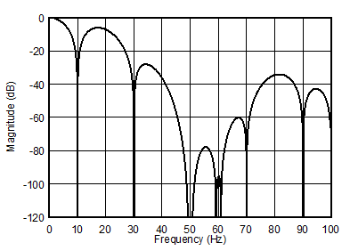
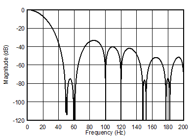
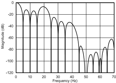
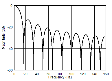
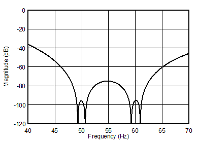
The low-latency filter provides many data rate options for rejecting 50-Hz and 60-Hz line cycle noise. At data rates of 2.5 SPS, 5 SPS, 10 SPS, and 20 SPS, the filter rejects both 50-Hz and 60-Hz line frequencies. At data rates of 16.6 SPS and 50 SPS, the filter has a notch at 50 Hz. At a 60-SPS data rate, the filter has a notch at 60 Hz.

For detailed frequency response plots showing line cycle noise rejection, download the ADS1x4S0x design calculator from www.ti.com.

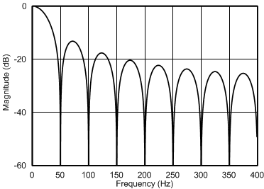
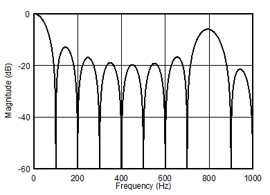
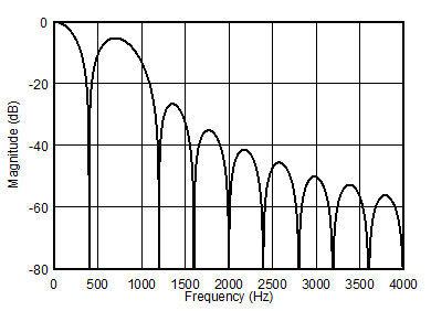
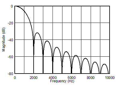
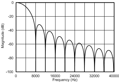
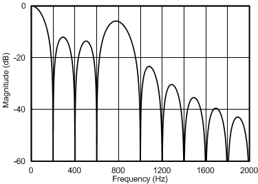
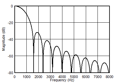
Figure 54 to Figure 68 show the frequency response of the low-latency filter for different data rates. Table 12 gives the bandwidth of the low-latency filter for each data rate.
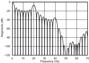
ADS114S06 ADS114S08 ai_ll_filt_2p5sps_sbas660.gif
fCLK = 4.096 MHz, low-latency filter
Figure 54. Low-Latency Filter Frequency Response,
Data Rate = 2.5 SPS
ADS114S06 ADS114S08 ai_ll_filt_10sps_sbas660.gif
fCLK = 4.096 MHz, low-latency filter
Figure 56. Low-Latency Filter Frequency Response,
Data Rate = 10 SPS
ADS114S06 ADS114S08 ai_ll_filt_20sps_sbas660.gif
fCLK = 4.096 MHz, low-latency filter
Figure 58. Low-Latency Filter Frequency Response,
Data Rate = 20 SPS
ADS114S06 ADS114S08 ai_ll_filt_50sps_sbas660.gif
fCLK = 4.096 MHz, low-latency filter
Figure 60. Low-Latency Filter Frequency Response,
Data Rate = 50 SPS
ADS114S06 ADS114S08 ai_ll_filt_100sps_sbas660.gif
fCLK = 4.096 MHz, low-latency filter
Figure 62. Low-Latency Filter Frequency Response,
Data Rate = 100 SPS
ADS114S06 ADS114S08 ai_ll_filt_400sps_sbas660.gif
fCLK = 4.096 MHz, low-latency filter
Figure 64. Low-Latency Filter Frequency Response,
Data Rate = 400 SPS
ADS114S06 ADS114S08 ai_ll_filt_1ksps_sbas660.gif
fCLK = 4.096 MHz, low-latency filter
Figure 66. Low-Latency Filter Frequency Response,
Data Rate = 1 kSPS
ADS114S06 ADS114S08 ai_ll_filt_4ksps_sbas660.gif
fCLK = 4.096 MHz, low-latency filter
Figure 68. Low-Latency Filter Frequency Response,
Data Rate = 4 kSPS
ADS114S06 ADS114S08 ai_ll_filt_5sps_sbas660.gif
fCLK = 4.096 MHz, low-latency filter
Figure 55. Low-Latency Filter Frequency Response,
Data Rate = 5 SPS
ADS114S06 ADS114S08 ai_ll_filt_16sps_sbas660.gif
fCLK = 4.096 MHz, low-latency filter
Figure 57. Low-Latency Filter Frequency Response,
Data Rate = 16.6 SPS
ADS114S06 ADS114S08 ai_ll_filt_20sps_50_60_sbas660.gif
fCLK = 4.096 MHz, low-latency filter
Figure 59. Low-Latency Filter Frequency Response,
Data Rate = 20 SPS, Zoomed to 50 Hz and 60 Hz
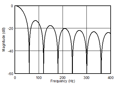
ADS114S06 ADS114S08 ai_ll_filt_60sps_sbas660.gif
fCLK = 4.096 MHz, low-latency filter
Figure 61. Low-Latency Filter Frequency Response,
Data Rate = 60 SPS
ADS114S06 ADS114S08 ai_ll_filt_200sps_sbas660.gif
fCLK = 4.096 MHz, low-latency filter
Figure 63. Low-Latency Filter Frequency Response,
Data Rate = 200 SPS
ADS114S06 ADS114S08 ai_ll_filt_800sps_sbas660.gif
fCLK = 4.096 MHz, low-latency filter
Figure 65. Low-Latency Filter Frequency Response,
Data Rate = 800 SPS
ADS114S06 ADS114S08 ai_ll_filt_2ksps_sbas660.gif
fCLK = 4.096 MHz, low-latency filter
Figure 67. Low-Latency Filter Frequency Response,
Data Rate = 2 kSPS

Table 12. Low-Latency Filter Bandwidth

NOMINAL DATA RATE (SPS)(1)–3-dB BANDWIDTH (Hz)(1)
2.5 1.1
5 2.2
10 4.7
16.6 7.4
20 13.2
50 22.1
60 26.6
100 44.4
200 89.9
400 190
800 574
1000 718
2000 718
4000 718
Valid for the internal oscillator or an external 4.096-MHz clock. Scales proportional with fCLK.

The low-latency filter notches and output data rate scale proportionally with the clock frequency. For example, a notch that appears at 20 Hz when using a 4.096-MHz clock appears at 10 Hz if a 2.048-MHz clock is used. Note that the internal oscillator can vary over temperature as specified in the Electrical Characteristics table. The data rate, conversion time, and filter notches consequently vary by the same percentage. Consider using an external precision clock source if a digital filter notch at a specific frequency with a tighter tolerance is required.