SBAS852A August   2017  – February 2020 ADS114S06B , ADS114S08B

PRODUCTION DATA.  

  1. Features
  2. Applications
  3. Description
    1.     Device Images
      1.      Functional Block Diagram
  4. Revision History
  5. Device Comparison Table
  6. Pin Configuration and Functions
    1.     Pin Functions
  7. Specifications
    1. 7.1 Absolute Maximum Ratings
    2. 7.2 ESD Ratings
    3. 7.3 Recommended Operating Conditions
    4. 7.4 Thermal Information
    5. 7.5 Electrical Characteristics
    6. 7.6 Timing Requirements
    7. 7.7 Switching Characteristics
    8. 7.8 Typical Characteristics
  8. Parameter Measurement Information
    1. 8.1 Noise Performance
  9. Detailed Description
    1. 9.1 Overview
    2. 9.2 Functional Block Diagram
    3. 9.3 Feature Description
      1. 9.3.1  Multiplexer
      2. 9.3.2  Low-Noise Programmable Gain Amplifier
        1. 9.3.2.1 PGA Input-Voltage Requirements
        2. 9.3.2.2 Bypassing the PGA
      3. 9.3.3  Voltage Reference
        1. 9.3.3.1 Internal Reference
        2. 9.3.3.2 External Reference
        3. 9.3.3.3 Reference Buffers
      4. 9.3.4  Clock Source
      5. 9.3.5  Delta-Sigma Modulator
      6. 9.3.6  Digital Filter
        1. 9.3.6.1 Digital Filter Frequency Response
        2. 9.3.6.2 Data Conversion Time
        3. 9.3.6.3 Note on Conversion Time
        4. 9.3.6.4 50-Hz and 60-Hz Line Cycle Rejection
      7. 9.3.7  Excitation Current Sources (IDACs)
      8. 9.3.8  Bias Voltage Generation
      9. 9.3.9  System Monitor
        1. 9.3.9.1 Internal Temperature Sensor
        2. 9.3.9.2 Power Supply Monitors
        3. 9.3.9.3 Burn-Out Current Sources
      10. 9.3.10 Status Register
        1. 9.3.10.1 POR Flag
        2. 9.3.10.2 RDY Flag
        3. 9.3.10.3 External Reference Monitor
      11. 9.3.11 General-Purpose Inputs and Outputs (GPIOs)
      12. 9.3.12 Calibration
        1. 9.3.12.1 Offset Calibration
        2. 9.3.12.2 Gain Calibration
    4. 9.4 Device Functional Modes
      1. 9.4.1 Reset
        1. 9.4.1.1 Power-On Reset
        2. 9.4.1.2 RESET Pin
        3. 9.4.1.3 Reset by Command
      2. 9.4.2 Power-Down Mode
      3. 9.4.3 Standby Mode
      4. 9.4.4 Conversion Modes
        1. 9.4.4.1 Continuous Conversion Mode
        2. 9.4.4.2 Single-Shot Conversion Mode
    5. 9.5 Programming
      1. 9.5.1 Serial Interface
        1. 9.5.1.1 Chip Select (CS)
        2. 9.5.1.2 Serial Clock (SCLK)
        3. 9.5.1.3 Serial Data Input (DIN)
        4. 9.5.1.4 Serial Data Output and Data Ready (DOUT/DRDY)
        5. 9.5.1.5 Data Ready (DRDY)
        6. 9.5.1.6 Timeout
      2. 9.5.2 Data Format
      3. 9.5.3 Commands
        1. 9.5.3.1  NOP
        2. 9.5.3.2  WAKEUP
        3. 9.5.3.3  POWERDOWN
        4. 9.5.3.4  RESET
        5. 9.5.3.5  START
        6. 9.5.3.6  STOP
        7. 9.5.3.7  SYOCAL
        8. 9.5.3.8  SYGCAL
        9. 9.5.3.9  SFOCAL
        10. 9.5.3.10 RDATA
        11. 9.5.3.11 RREG
        12. 9.5.3.12 WREG
      4. 9.5.4 Interfacing with Multiple Devices
    6. 9.6 Register Map
      1. 9.6.1 Configuration Registers
      2. 9.6.2 Register Descriptions
        1. 9.6.2.1  Device ID Register (address = 00h) [reset = xxh]
          1. Table 16. Device ID (ID) Register Field Descriptions
        2. 9.6.2.2  Device Status Register (address = 01h) [reset = 80h]
          1. Table 17. Device Status (STATUS) Register Field Descriptions
        3. 9.6.2.3  Input Multiplexer Register (address = 02h) [reset = 01h]
          1. Table 18. Input Multiplexer (INPMUX) Register Field Descriptions
        4. 9.6.2.4  Gain Setting Register (address = 03h) [reset = 00h]
          1. Table 19. Gain Setting (PGA) Register Field Descriptions
        5. 9.6.2.5  Data Rate Register (address = 04h) [reset = 14h]
          1. Table 20. Data Rate (DATARATE) Register Field Descriptions
        6. 9.6.2.6  Reference Control Register (address = 05h) [reset = 10h]
          1. Table 21. Reference Control (REF) Register Field Descriptions
        7. 9.6.2.7  Excitation Current Register 1 (address = 06h) [reset = 00h]
          1. Table 22. Excitation Current Register 1 (IDACMAG) Register Field Descriptions
        8. 9.6.2.8  Excitation Current Register 2 (address = 07h) [reset = FFh]
          1. Table 23. Excitation Current Register 2 (IDACMUX) Register Field Descriptions
        9. 9.6.2.9  Sensor Biasing Register (address = 08h) [reset = 00h]
          1. Table 24. Sensor Biasing (VBIAS) Register Field Descriptions
        10. 9.6.2.10 System Control Register (address = 09h) [reset = 10h]
          1. Table 25. System Control (SYS) Register Field Descriptions
        11. 9.6.2.11 Reserved Register (address = 0Ah) [reset = 00h]
          1. Table 26. Reserved Register Field Descriptions
        12. 9.6.2.12 Offset Calibration Register 1 (address = 0Bh) [reset = 00h]
          1. Table 27. Offset Calibration Register 1 (OFCAL0) Register Field Descriptions
        13. 9.6.2.13 Offset Calibration Register 2 (address = 0Ch) [reset = 00h]
          1. Table 28. Offset Calibration Register 2 (OFCAL1) Register Field Descriptions
        14. 9.6.2.14 Reserved Register (address = 0Dh) [reset = 00h]
          1. Table 29. Reserved Register Field Descriptions
        15. 9.6.2.15 Gain Calibration Register 1 (address = 0Eh) [reset = 00h]
          1. Table 30. Gain Calibration Register 1 (FSCAL0) Field Descriptions
        16. 9.6.2.16 Gain Calibration Register 2 (address = 0Fh) [reset = 40h]
          1. Table 31. Gain Calibration Register 2 (FSCAL1) Field Descriptions
        17. 9.6.2.17 GPIO Data Register (address = 10h) [reset = 00h]
          1. Table 32. GPIO Data (GPIODAT) Register Field Descriptions
        18. 9.6.2.18 GPIO Configuration Register (address = 11h) [reset = 00h]
          1. Table 33. GPIO Configuration (GPIOCON) Register Field Descriptions
  10. 10Application and Implementation
    1. 10.1 Application Information
      1. 10.1.1 Serial Interface Connections
      2. 10.1.2 Analog Input Filtering
      3. 10.1.3 External Reference and Ratiometric Measurements
      4. 10.1.4 Establishing a Proper Input Voltage
      5. 10.1.5 Unused Inputs and Outputs
      6. 10.1.6 Pseudo Code Example
    2. 10.2 Typical Application
      1. 10.2.1 Design Requirements
      2. 10.2.2 Detailed Design Procedure
        1. 10.2.2.1 Register Settings
      3. 10.2.3 Application Curves
    3. 10.3 What To Do and What Not To Do
  11. 11Power Supply Recommendations
    1. 11.1 Power Supplies
    2. 11.2 Power-Supply Sequencing
    3. 11.3 Power-On Reset
    4. 11.4 Power-Supply Decoupling
  12. 12Layout
    1. 12.1 Layout Guidelines
    2. 12.2 Layout Example
  13. 13Device and Documentation Support
    1. 13.1 Device Support
      1. 13.1.1 Development Support
    2. 13.2 Documentation Support
      1. 13.2.1 Related Documentation
    3. 13.3 Related Links
    4. 13.4 Receiving Notification of Documentation Updates
    5. 13.5 Community Resources
    6. 13.6 Trademarks
    7. 13.7 Electrostatic Discharge Caution
    8. 13.8 Glossary
  14. 14Mechanical, Packaging, and Orderable Information

Package Options

Refer to the PDF data sheet for device specific package drawings

Mechanical Data (Package|Pins)
  • RHB|32
  • PBS|32
Thermal pad, mechanical data (Package|Pins)
Orderable Information

Excitation Current Sources (IDACs)

The ADS114S0xB incorporates two integrated, matched current sources (IDAC1, IDAC2). The current sources provide excitation current to resistive temperature devices (RTDs), thermistors, diodes, and other resistive sensors that require constant current biasing. The current sources are programmable to output values between 10 μA to 2000 μA using the IMAG[3:0] bits in the excitation current register 1 (06h). Each current source can be connected to any of the analog inputs AINx as well as the REFP1 and REFN1 inputs for the ADS114S06B. Both current sources can also be connected to the same pin. The routing of the IDACs is configured by the I1MUX[3:0] and I2MUX[3:0] bits in the excitation current register 2 (07h). In three-wire RTD applications, the matched current sources can be used to cancel errors caused by sensor lead resistance (see the Typical Application section for more details). Figure 63 details the IDAC connection through the input multiplexer.
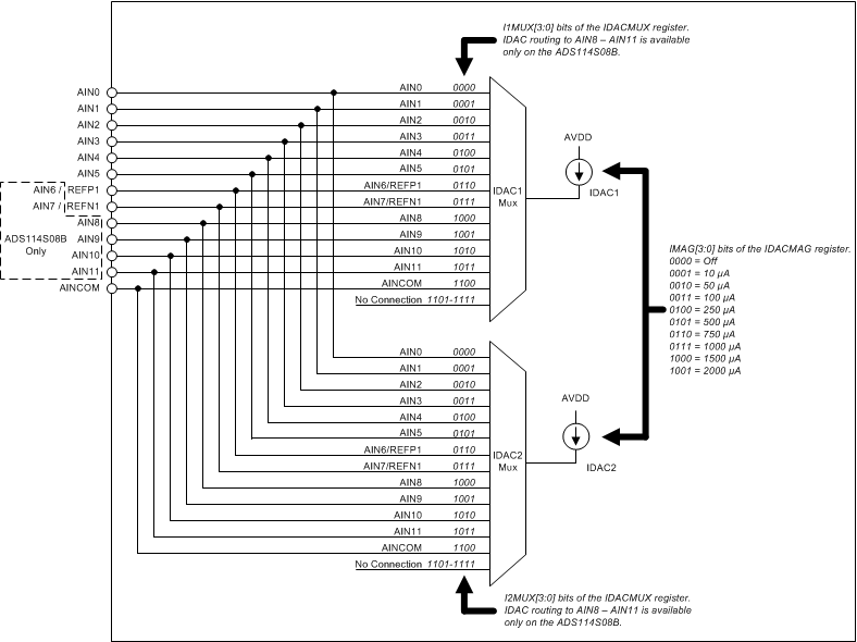
ADS114S06B ADS114S08B ai_idac_bd_sbas852.gifFigure 63. IDAC Block Diagram

The internal reference must be enabled for IDAC operation. As with any current source, the IDAC requires voltage headroom to the positive supply to operate. This voltage headroom is the compliance voltage. When driving resistive sensors and biasing resistors, take care not to exceed the compliance voltage of the IDACs, otherwise the specified accuracy of the IDAC current may not be met. For IDAC compliance voltage specifications, see the Electrical Characteristics table.