SBAS435 September 2017 ADS1287D
PRODUCTION DATA.
- 1Features
- 2Applications
- 3Description
- 4Device and Documentation Support
- 5Mechanical, Packaging, and Orderable Information
Package Options
Mechanical Data (Package|Pins)
- RHB|32
Thermal pad, mechanical data (Package|Pins)
Orderable Information
1 Features
- SNR: 114 dB (50 Hz–200 Hz, Gain = 1)
- Power: 2.2 mW (Per ADC)
- THD: –115 dB
- CMRR: 110 dB
- High-Impedance CMOS PGA:
- Gains 1, 2, 4, 8, and 16
- Data Rates: 62.5 SPS to 1000 SPS
- Flexible Digital Filter:
- Sinc + FIR + IIR (Selectable)
- Linear and Minimum Phase Response
- Programmable High-Pass Filter
- Sensor-Test Current Sources
- Offset and Gain Calibration
- Synchronization Control
- SPI™-Compatible Interface
- Analog Power Supply: 5 V or ±2.5 V
- Digital Power Supply: 2.5 V to 3.3 V
2 Applications
- Energy Exploration
- Passive Seismic Monitoring
- Portable Instrumentation
3 Description
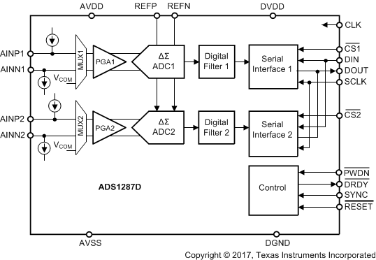
The ADS1287D device is a dual, simultaneous-sampling, analog-to-digital converter (ADC), with an integrated programmable gain amplifier (PGA) and finite-impulse-response (FIR) digital filter. The ADC is suitable for the demanding needs of low-power, seismic data acquisition.
The ADC features a programmable-gain, high-impedance amplifier suitable for direct connection of geophone and hydrophone sensors to the ADC over a wide range of input signals (±2.5 V to ±0.156 V). Dual 100-nA current sources are integrated into the ADC inputs for field testing of sensors.
The ADC incorporates a fourth-order, inherently stable, delta-sigma (ΔΣ) modulator. The modulator digital output is filtered and decimated by the internal FIR digital filter to yield the ADC conversion result.
The FIR digital filter provides data rates up to 1000 samples per second (SPS). The high-pass filter (HPF) removes DC and low-frequency components from the conversion result. On-chip gain and offset scaling registers support system calibration.
Total device power consumption is 4.4 mW. The ADC is packaged in a compact 5-mm × 5-mm VQFN package and is fully specified over the –40°C to +85°C temperature range.
Device Information(1)
| PART NUMBER | PACKAGE | BODY SIZE (NOM) |
|---|---|---|
| ADS1287D | VQFN (32) | 5.00 mm × 5.00 mm |
- For all available packages, see the package option addendum at the end of the data sheet.
Functional Block Diagram
