SBAS499C July 2012 – January 2017 ADS1299 , ADS1299-4 , ADS1299-6
PRODUCTION DATA.
- 1 Features
- 2 Applications
- 3 Description
- 4 Revision History
- 5 Device Comparison
- 6 Pin Configuration and Functions
- 7 Specifications
- 8 Parametric Measurement Information
-
9 Detailed Description
- 9.1 Overview
- 9.2 Functional Block Diagram
- 9.3
Feature Description
- 9.3.1 Analog Functionality
- 9.3.2
Digital Functionality
- 9.3.2.1 Digital Decimation Filter
- 9.3.2.2 Clock
- 9.3.2.3 GPIO
- 9.3.2.4 ECG and EEG Specific Features
- 9.4 Device Functional Modes
- 9.5
Programming
- 9.5.1 Data Format
- 9.5.2 SPI Interface
- 9.5.3
SPI Command Definitions
- 9.5.3.1 Sending Multi-Byte Commands
- 9.5.3.2 WAKEUP: Exit STANDBY Mode
- 9.5.3.3 STANDBY: Enter STANDBY Mode
- 9.5.3.4 RESET: Reset Registers to Default Values
- 9.5.3.5 START: Start Conversions
- 9.5.3.6 STOP: Stop Conversions
- 9.5.3.7 RDATAC: Read Data Continuous
- 9.5.3.8 SDATAC: Stop Read Data Continuous
- 9.5.3.9 RDATA: Read Data
- 9.5.3.10 RREG: Read From Register
- 9.5.3.11 WREG: Write to Register
- 9.6
Register Maps
- 9.6.1
User Register Description
- 9.6.1.1 ID: ID Control Register (address = 00h) (reset = xxh)
- 9.6.1.2 CONFIG1: Configuration Register 1 (address = 01h) (reset = 96h)
- 9.6.1.3 CONFIG2: Configuration Register 2 (address = 02h) (reset = C0h)
- 9.6.1.4 CONFIG3: Configuration Register 3 (address = 03h) (reset = 60h)
- 9.6.1.5 LOFF: Lead-Off Control Register (address = 04h) (reset = 00h)
- 9.6.1.6 CHnSET: Individual Channel Settings (n = 1 to 8) (address = 05h to 0Ch) (reset = 61h)
- 9.6.1.7 BIAS_SENSP: Bias Drive Positive Derivation Register (address = 0Dh) (reset = 00h)
- 9.6.1.8 BIAS_SENSN: Bias Drive Negative Derivation Register (address = 0Eh) (reset = 00h)
- 9.6.1.9 LOFF_SENSP: Positive Signal Lead-Off Detection Register (address = 0Fh) (reset = 00h)
- 9.6.1.10 LOFF_SENSN: Negative Signal Lead-Off Detection Register (address = 10h) (reset = 00h)
- 9.6.1.11 LOFF_FLIP: Lead-Off Flip Register (address = 11h) (reset = 00h)
- 9.6.1.12 LOFF_STATP: Lead-Off Positive Signal Status Register (address = 12h) (reset = 00h)
- 9.6.1.13 LOFF_STATN: Lead-Off Negative Signal Status Register (address = 13h) (reset = 00h)
- 9.6.1.14 GPIO: General-Purpose I/O Register (address = 14h) (reset = 0Fh)
- 9.6.1.15 MISC1: Miscellaneous 1 Register (address = 15h) (reset = 00h)
- 9.6.1.16 MISC2: Miscellaneous 2 (address = 16h) (reset = 00h)
- 9.6.1.17 CONFIG4: Configuration Register 4 (address = 17h) (reset = 00h)
- 9.6.1
User Register Description
- 10Applications and Implementation
- 11Power Supply Recommendations
- 12Layout
- 13Device and Documentation Support
- 14Mechanical, Packaging, and Orderable Information
Package Options
Mechanical Data (Package|Pins)
- PAG|64
Thermal pad, mechanical data (Package|Pins)
- PAG|64
Orderable Information
7 Specifications
7.1 Absolute Maximum Ratings(1)
| MIN | MAX | UNIT | ||
|---|---|---|---|---|
| Voltage | AVDD to AVSS | –0.3 | 5.5 | V |
| DVDD to DGND | –0.3 | 3.9 | ||
| AVSS to DGND | –3 | 0.2 | ||
| VREFP to AVSS | –0.3 | AVDD + 0.3 | ||
| VREFN to AVSS | –0.3 | AVDD + 0.3 | ||
| Analog input | AVSS – 0.3 | AVDD + 0.3 | ||
| Digital input | DGND – 0.3 | DVDD + 0.3 | ||
| Current | Input, continuous, any pin except power supply pins(2) | –10 | 10 | mA |
| Temperature | Junction, TJ | 150 | °C | |
| Storage, Tstg | –60 | 150 | ||
(1) Stresses beyond those listed under Absolute Maximum Ratings may cause permanent damage to the device. These are stress ratings only, which do not imply functional operation of the device at these or any other conditions beyond those indicated under Recommended Operating Conditions. Exposure to absolute-maximum-rated conditions for extended periods may affect device reliability.
(2) Input pins are diode-clamped to the power-supply rails. Limit the input current to 10 mA or less if the analog input voltage exceeds AVDD + 0.3 V or is less than AVSS – 0.3 V, or if the digital input voltage exceeds DVDD + 0.3 V or is less than DGND – 0.3 V.
7.2 ESD Ratings
| VALUE | UNIT | |||
|---|---|---|---|---|
| V(ESD) | Electrostatic discharge | Human-body model (HBM), per ANSI/ESDA/JEDEC JS-001(1) | ±1000 | V |
| Charged-device model (CDM), per JEDEC specification JESD22-C101(2) | ±500 | |||
(1) JEDEC document JEP155 states that 500-V HBM allows safe manufacturing with a standard ESD control process.
(2) JEDEC document JEP157 states that 250-V CDM allows safe manufacturing with a standard ESD control process.
7.3 Recommended Operating Conditions
over operating ambient temperature range (unless otherwise noted)| MIN | NOM | MAX | UNIT | |||
|---|---|---|---|---|---|---|
| POWER SUPPLY | ||||||
| Analog power supply | AVDD to AVSS | 4.75 | 5 | 5.25 | V | |
| Digital power supply | DVDD to DGND | 1.8 | 1.8 | 3.6 | V | |
| Analog to Digital supply | AVDD – DVDD | –2.1 | 3.6 | V | ||
| ANALOG INPUTS | ||||||
| Full-scale differential input voltage | VINxP – VINxN | ±VREF / gain | V | |||
| VCM | Input common-mode range | (VINxP + VINxN) / 2 | See the Input Common-Mode Range subsection of the PGA Settings and Input Range section | |||
| VOLTAGE REFERENCE INPUTS | ||||||
| VREF | Reference input voltage | VREF = (VVREFP – VVREFN) | 4.5 | V | ||
| VREFN | Negative input | AVSS | V | |||
| VREFP | Positive input | AVSS + 4.5 | V | |||
| CLOCK INPUT | ||||||
| fCLK | External clock input frequency | CLKSEL pin = 0 | 1.5 | 2.048 | 2.25 | MHz |
| DIGITAL INPUTS | ||||||
| Input voltage | DGND – 0.1 | DVDD + 0.1 | V | |||
| TEMPERATURE RANGE | ||||||
| TA | Operating temperature range | –40 | 85 | °C | ||
7.4 Thermal Information
| THERMAL METRIC(1) | ADS1299-4, ADS1299-6, ADS1299 | UNIT | |
|---|---|---|---|
| PAG (TQFP) | |||
| 64 PINS | |||
| RθJA | Junction-to-ambient thermal resistance | 46.2 | °C/W |
| RθJC(top) | Junction-to-case (top) thermal resistance | 5.8 | °C/W |
| RθJB | Junction-to-board thermal resistance | 19.6 | °C/W |
| ψJT | Junction-to-top characterization parameter | 0.2 | °C/W |
| ψJB | Junction-to-board characterization parameter | 19.2 | °C/W |
| RθJC(bot) | Junction-to-case (bottom) thermal resistance | n/a | °C/W |
(1) For more information about traditional and new thermal metrics, see the Semiconductor and IC Package Thermal Metrics application report.
7.5 Electrical Characteristics
Minimum and maximum specifications apply from TA = –40°C to 85°C. Typical specifications are at TA = +25°C. All specifications are at AVDD – AVSS = 5 V, DVDD = 3.3 V, VREF = 4.5 V, external fCLK = 2.048 MHz, data rate = 250 SPS, and gain = 12 (unless otherwise noted)| PARAMETER | TEST CONDITIONS | MIN | TYP | MAX | UNIT | ||
|---|---|---|---|---|---|---|---|
| ANALOG INPUTS | |||||||
| Input capacitance | 20 | pF | |||||
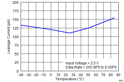
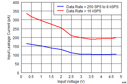
| Input bias current | TA = +25°C, InxP and INxN = 2.5 V | ±300 | pA | ||||
| TA = –40°C to +85°C, InxP and INxN = 2.5 V | ±300 | ||||||
| DC input impedance | No lead-off | 1000 | MΩ | ||||
| Current source lead-off detection (ILEADOFF = 6 nA) |
500 | ||||||
| PGA PERFORMANCE | |||||||
| Gain settings | 1, 2, 4, 6, 8, 12, 24 | ||||||
| BW | Bandwidth | See Table 5 | |||||
| ADC PERFORMANCE | |||||||
| Resolution | 24 | Bits | |||||
| DR | Data rate | fCLK = 2.048 MHz | 250 | 16000 | SPS | ||
| DC CHANNEL PERFORMANCE | |||||||
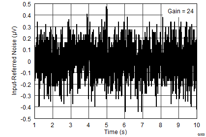
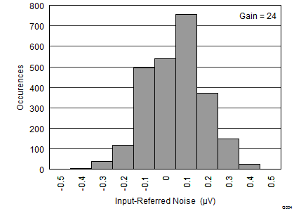
| Input-referred noise (0.01 Hz to 70 Hz) | 10 seconds of data, gain = 24(1) | 1 | μVPP | ||||
| 250 points, 1 second of data, gain = 24, TA = +25°C | 1 | 1.35 | |||||
| 250 points, 1 second of data, gain = 24, TA = –40°C to +85°C | 1 | 1.6 | |||||
| All other sample rates and gain settings | See Noise Measurements | ||||||
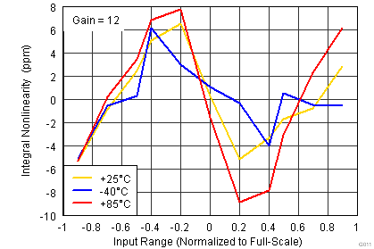
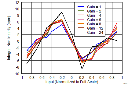
| INL | Integral nonlinearity | Full-scale with gain = 12, best fit | 8 | ppm | |||
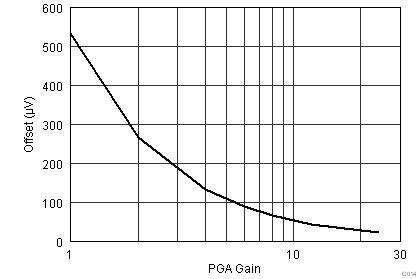
| Offset error | 60 | μV | |||||
| Offset error drift | 80 | nV/°C | |||||
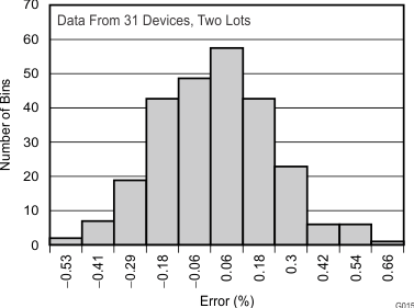
| Gain error | Excluding voltage reference error | 0.1 | ±0.5 | % of FS | |||
| Gain drift | Excluding voltage reference drift | 3 | ppm/°C | ||||
| Gain match between channels | 0.2 | % of FS | |||||
| AC CHANNEL PERFORMANCE | |||||||
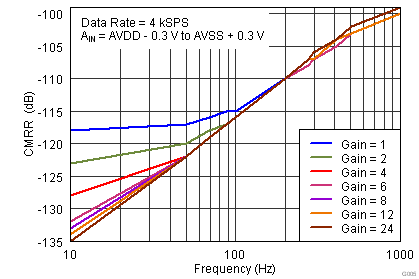
| CMRR | Common-mode rejection ratio | fCM = 50 Hz and 60 Hz(2) | –110 | –120 | dB | ||
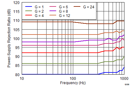
| PSRR | Power-supply rejection ratio | fPS = 50 Hz and 60 Hz | 96 | dB | |||
| Crosstalk | fIN = 50 Hz and 60 Hz | –110 | dB | ||||
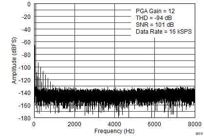
| SNR | Signal-to-noise ratio | VIN = –2 dBFs, fIN = 10-Hz input, gain = 12 | 121 | dB | |||
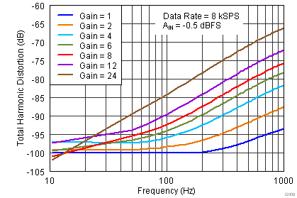
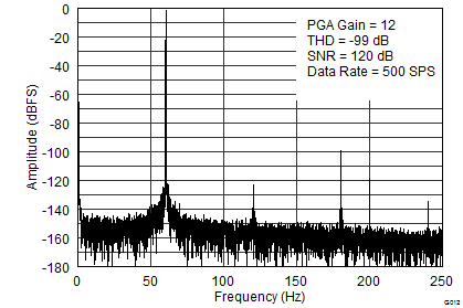
| THD | Total harmonic distortion | VIN = –0.5 dBFs, fIN = 10 Hz | –99 | dB | |||
| PATIENT BIAS AMPLIFIER | |||||||
| Integrated noise | BW = 150 Hz | 2 | μVRMS | ||||
| Gain bandwidth product | 50-kΩ || 10-pF load, gain = 1 | 100 | kHz | ||||
| Slew rate | 50-kΩ || 10-pF load, gain = 1 | 0.07 | V/μs | ||||
| THD | Total harmonic distortion | fIN = 10 Hz, gain = 1 | –80 | dB | |||
| Common-mode input range | AVSS + 0.3 | AVDD – 0.3 | V | ||||
| Short-circuit current | 1.1 | mA | |||||
| Quiescent power consumption | 20 | μA | |||||
| LEAD-OFF DETECT | |||||||
| Frequency | Continuous | At dc, fDR / 4, see Register Maps for settings |
Hz | ||||
| One time or periodic | 7.8, 31.2 | ||||||
| Current | ILEAD_OFF[1:0] = 00 | 6 | nA | ||||
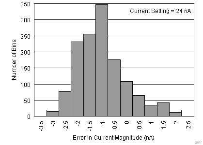
| ILEAD_OFF[1:0] = 01 | 24 | ||||||
| ILEAD_OFF[1:0] = 10 | 6 | μA | |||||
| ILEAD_OFF[1:0] = 11 | 24 | ||||||
| Current accuracy | ±20% | ||||||
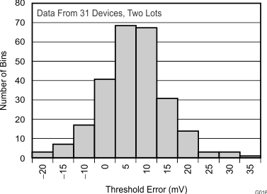
| Comparator threshold accuracy | ±30 | mV | |||||
| EXTERNAL REFERENCE | |||||||
| Input impedance | 5.6 | kΩ | |||||
| INTERNAL REFERENCE | |||||||
| VREF | Internal reference voltage | 4.5 | V | ||||
| VREF accuracy | ±0.2% | ||||||
| Drift | TA = –40°C to +85°C | 35 | ppm/°C | ||||
| Start-up time | 150 | ms | |||||
| SYSTEM MONITORS | |||||||
| Reading error | Analog supply | 2% | |||||
| Digital supply | 2% | ||||||
| Device wake up | From power-up to DRDY low | 150 | ms | ||||
| STANDBY mode | 31.25 | µs | |||||
| Temperature sensor reading | Voltage | TA = +25°C | 145 | mV | |||
| Coefficient | 490 | μV/°C | |||||
| Test signal | Signal frequency | See Register Maps section for settings | fCLK / 221, fCLK / 220 | Hz | |||
| Signal voltage | See Register Maps section for settings | ±1, ±2 | mV | ||||
| Accuracy | ±2% | ||||||
| CLOCK | |||||||
| Internal oscillator clock frequency | Nominal frequency | 2.048 | MHz | ||||
| Internal clock accuracy | TA = +25°C | ±0.5% | |||||
| TA = –40°C to +85°C | ±2.5% | ||||||
| Internal oscillator start-up time | 20 | μs | |||||
| Internal oscillator power consumption | 120 | μW | |||||
| DIGITAL INPUT/OUTPUT (DVDD = 1.8 V to 3.6 V) | |||||||
| VIH | High-level input voltage | 0.8 DVDD | DVDD + 0.1 | V | |||
| VIL | Low-level input voltage | –0.1 | 0.2 DVDD | V | |||
| VOH | High-level output voltage | IOH = –500 μA | 0.9 DVDD | V | |||
| VOL | Low-level output voltage | IOL = +500 μA | 0.1 DVDD | V | |||
| Input current | 0 V < VDigitalInput < DVDD | –10 | 10 | μA | |||
| SUPPLY CURRENT (Bias Turned Off) | |||||||
| IAVDD | AVDD current | ADS1299-4 | Normal mode, AVDD – AVSS = 5 V | 4.06 | mA | ||
| ADS1299-6 | 5.57 | ||||||
| ADS1299 | 7.14 | ||||||
| IDVDD | DVDD current | ADS1299-4 | Normal mode, DVDD = 3.3 V | 0.54 | mA | ||
| ADS1299-6 | 0.66 | ||||||
| ADS1299 | 1 | ||||||
| ADS1299-4 | Normal mode, DVDD = 1.8 V | 0.27 | |||||
| ADS1299-6 | 0.34 | ||||||
| ADS1299 | 0.5 | ||||||
| POWER DISSIPATION (Analog Supply = 5 V, Bias Amplifiers Turned Off) | |||||||
| Power dissipation | ADS1299-4 | Normal mode | 22 | 24 | mW | ||
| Power-down | 10 | µW | |||||
| Standby mode, internal reference | 5.1 | mW | |||||
| ADS1299-6 | Normal mode | 30 | 33 | mW | |||
| Power-down | 10 | µW | |||||
| Standby mode, internal reference | 5.1 | mW | |||||
| ADS1299 | Normal mode | 39 | 42 | mW | |||
| Power-down | 10 | µW | |||||
| Standby mode, internal reference | 5.1 | mW | |||||
(1) Noise data measured in a 10-second interval. Test not performed in production. Input-referred noise is calculated with the input shorted (without electrode resistance) over a 10-second interval.
(2) CMRR is measured with a common-mode signal of AVSS + 0.3 V to AVDD – 0.3 V. The values indicated are the minimum of the eight channels.
7.6 Timing Requirements: Serial Interface
over operating ambient temperature range (unless otherwise noted)7.7 Switching Characteristics: Serial Interface
over operating ambient temperature range (unless otherwise noted)| PARAMETER | 2.7 V ≤ DVDD ≤ 3.6 V | 1.8 V ≤ DVDD ≤ 2.0 V | UNIT | |||
|---|---|---|---|---|---|---|
| MIN | MAX | MIN | MAX | |||
| tDOHD | Hold time, SCLK falling edge to invalid DOUT | 10 | 10 | ns | ||
| tDOPD | Propagation delay time, SCLK rising edge to DOUT valid | 17 | 32 | ns | ||
| tCSDOD | Propagation delay time, CS low to DOUT driven | 10 | 20 | ns | ||
| tCSDOZ | Propagation delay time, CS high to DOUT Hi-Z | 10 | 20 | ns | ||
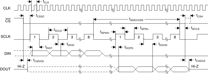
NOTE:
SPI settings are CPOL = 0 and CPHA = 1. Figure 2. Daisy-Chain Interface Timing
7.8 Typical Characteristics
At TA = 25°C, AVDD = 5 V, AVSS = 0 V, DVDD = 3.3 V, internal VREFP = 4.5 V, VREFN = AVSS, external clock = 2.048 MHz, data rate = 250 SPS, and gain = 12 (unless otherwise noted)