SBAS608C June 2014 – December 2015 ADS7042
PRODUCTION DATA.
- 1 Features
- 2 Applications
- 3 Description
- 4 Revision History
- 5 Companion Products
- 6 Device Comparison
- 7 Pin Configuration and Functions
- 8 Specifications
- 9 Parameter Measurement Information
- 10Detailed Description
- 11Application and Implementation
- 12Power-Supply Recommendations
- 13Layout
- 14Device and Documentation Support
- 15Mechanical, Packaging, and Orderable Information
Package Options
Refer to the PDF data sheet for device specific package drawings
Mechanical Data (Package|Pins)
- DCU|8
- RUG|8
Thermal pad, mechanical data (Package|Pins)
Orderable Information
13 Layout
13.1 Layout Guidelines
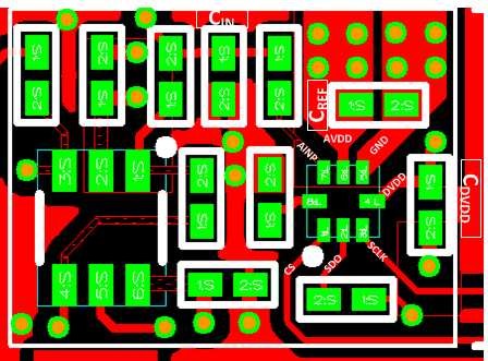
Figure 47 shows a board layout example for the ADS7042. Use a ground plane underneath the device and partition the PCB into analog and digital sections. Avoid crossing digital lines with the analog signal path and keep the analog input signals and the reference input signals away from noise sources. In Figure 47, the analog input and reference signals are routed on the top and left side of the device and the digital connections are routed on the bottom and right side of the device.
The power sources to the device must be clean and well-bypassed. Use 1-μF ceramic bypass capacitors in close proximity to the analog (AVDD) and digital (DVDD) power-supply pins. Avoid placing vias between the AVDD and DVDD pins and the bypass capacitors. Connect all ground pins to the ground plane using short, low-impedance paths. The AVDD supply voltage for the ADS7042 also functions as a reference for the device. Place the decoupling capacitor (CREF) for AVDD close to the device AVDD and GND pins and connect CREF to the device pins with thick copper tracks, as shown in Figure 47.
The fly-wheel RC filters are placed close to the device. Among ceramic surface-mount capacitors, COG (NPO) ceramic capacitors provide the best capacitance precision. The type of dielectric used in COG (NPO) ceramic capacitors provides the most stable electrical properties over voltage, frequency, and temperature changes.
13.2 Layout Example
 Figure 47. Example Layout