SBAS584B October 2013 – August 2014 ADS7253 , ADS7853 , ADS8353
PRODUCTION DATA.
- 1 Features
- 2 Applications
- 3 Description
- 4 Revision History
- 5 Device Comparison Table
- 6 Pin Configurations and Functions
-
7 Specifications
- 7.1 Absolute Maximum Ratings
- 7.2 Handling Ratings
- 7.3 Recommended Operating Conditions
- 7.4 Thermal Information
- 7.5 Electrical Characteristics: ADS8353
- 7.6 Electrical Characteristics: ADS7853
- 7.7 Electrical Characteristics: ADS7253
- 7.8 Electrical Characteristics: All Devices
- 7.9 Timing Requirements: Interface Mode
- 7.10 Timing Characteristics: Serial Interface
- 7.11 Typical Characteristics: ADS8353
- 7.12 Typical Characteristics: ADS7853
- 7.13 Typical Characteristics: ADS7253
- 7.14 Typical Characteristics: Common to ADS8353, ADS7853, and ADS7253
-
8 Detailed Description
- 8.1 Overview
- 8.2 Functional Block Diagram
- 8.3 Feature Description
- 8.4 Device Functional Modes
- 8.5 Register Maps and Serial Interface
- 9 Application and Implementation
- 10Power-Supply Recommendations
- 11Layout
- 12Device and Documentation Support
- 13Mechanical, Packaging, and Orderable Information
Package Options
Mechanical Data (Package|Pins)
Thermal pad, mechanical data (Package|Pins)
- RTE|16
Orderable Information
9 Application and Implementation
9.1 Application Information
The two primary circuits required to maximize the performance of a high-precision, successive approximation register (SAR), analog-to-digital converter (ADC) are the input driver and the reference driver circuits. This section details some general principles for designing these circuits, and some application circuits designed using these devices.
The device supports operation either with an internal or external reference source. Refer to the Reference section for details about the decoupling requirements.
The reference source to the ADC must provide low-drift and very accurate dc voltage and support the dynamic charge requirements without affecting the noise and linearity performance of the device. The output broadband noise (typically in the order of a few 100 μVRMS) of the reference source must be appropriately filtered by using a low-pass filter with a cutoff frequency of a few hundred hertz. After band-limiting the noise from the reference source, the next important step is to design a reference buffer that can drive the dynamic load posed by the reference input of the ADC. At the start of each conversion, the reference buffer must regulate the voltage of the reference pin within 1 LSB of the intended value. This condition necessitates the use of a large filter capacitor at the reference pin of the ADC. The amplifier selected to drive the reference input pin must be stable while driving this large capacitor and should have low output impedance, low offset, and temperature drift specifications. To reduce the dynamic current requirements and crosstalk between the channels, a separate reference buffer is recommended for driving the reference input of each ADC channel.
The input driver circuit for a high-precision ADC mainly consists of two parts: a driving amplifier and a fly-wheel RC filter. The amplifier is used for signal conditioning of the input voltage and its low output impedance provides a buffer between the signal source and the switched capacitor inputs of the ADC. The RC filter helps attenuate the sampling charge injection from the switched-capacitor input stage of the ADC and functions as an antialiasing filter to band-limit the wideband noise contributed by the front-end circuit. Careful design of the front-end circuit is critical to meet the linearity and noise performance of a high-precision ADC.
9.1.1 Input Amplifier Selection
Selection criteria for the input amplifiers is highly dependent on the input signal type and the performance goals of the data acquisition system. Some key amplifier specifications to consider while selecting an appropriate amplifier to drive the inputs of the ADC are:
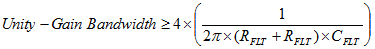
- Small-signal bandwidth. Select the small-signal bandwidth of the input amplifiers to be as high as possible after meeting the power budget of the system. Higher bandwidth reduces the closed-loop output impedance of the amplifier, thus allowing the amplifier to more easily drive the low cutoff frequency RC filter at the ADC inputs. Higher bandwidth also minimizes the harmonic distortion at higher input frequencies. In order to maintain the overall stability of the input driver circuit, the amplifier bandwidth should be selected as described in Equation 6:
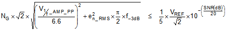
- Noise. Noise contribution of the front-end amplifiers should be as low as possible to prevent any degradation in SNR performance of the system. As a rule of thumb, to ensure that the noise performance of the data acquisition system is not limited by the front-end circuit, the total noise contribution from the front-end circuit should be kept below 20% of the input-referred noise of the ADC. Noise from the input driver circuit is band-limited by designing a low cutoff frequency RC filter and is calculated by Equation 7:
- V1 / f_AMP_PP is the peak-to-peak flicker noise in µV,
- en_RMS is the amplifier broadband noise density in nV/√Hz,
- f–3dB is the 3-dB bandwidth of the RC filter, and
- NG is the noise gain of the front-end circuit, which is equal to 1 in a buffer configuration.
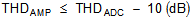
- Distortion. Both the ADC and the input driver introduce nonlinearity in a data acquisition block. As a rule of thumb, to ensure that the distortion performance of the data acquisition system is not limited by the front-end circuit, the distortion of the input driver should be at least 10 dB lower than the distortion of the ADC, as shown in Equation 8.
- Settling Time. For dc signals with fast transients that are common in a multiplexed application, the input signal must settle to the desired accuracy at the inputs of the ADC during the acquisition time window. This condition is critical to maintain the overall linearity performance of the ADC. Typically, the amplifier data sheets specify the output settling performance only up to 0.1% to 0.001%, which may not be sufficient for the desired accuracy. Therefore, the settling behavior of the input driver should always be verified by TINA™-SPICE simulations before selecting the amplifier.
where
9.1.2 Antialiasing Filter
Converting analog-to-digital signals requires sampling an input signal at a constant rate. Any higher frequency content in the input signal beyond half the sampling frequency is digitized and folded back into the low-frequency spectrum. This process is called aliasing. Therefore, an analog, antialiasing filter must be used to remove the harmonic content from the input signal before being sampled by the ADC. An antialiasing filter is designed as a low-pass, RC filter, for which the 3-dB bandwidth is optimized based on specific application requirements. For dc signals with fast transients (including multiplexed input signals), a high-bandwidth filter is designed to allow accurately settling the signal at the ADC inputs during the small acquisition time window. For ac signals, the filter bandwidth should be kept low to band-limit the noise fed into the ADC input, thereby increasing the signal-to-noise ratio (SNR) of the system.
A filter capacitor, CFLT, connected across the ADC inputs (as shown in Figure 100), filters the noise from the front-end drive circuitry, reduces the sampling charge injection and provides a charge bucket to quickly charge the internal sample-and-hold capacitors during the acquisition process. As a rule of thumb, the value of this capacitor should be at least 10 times the specified value of the ADC sampling capacitance. For these devices, the input sampling capacitance is equal to 40 pF. Thus, the value of CFLT should be greater than 400 pF. The capacitor should be a COG- or NPO-type because these capacitor types have a high-Q, low-temperature coefficient, and stable electrical characteristics under varying voltages, frequency, and time.
Note that driving capacitive loads can degrade the phase margin of the input amplifiers, thus making the amplifier marginally unstable. To avoid amplifier stability issues, series isolation resistors (RFLT) are used at the output of the amplifiers. A higher value of RFLT is helpful from the amplifier stability perspective, but adds distortion as a result of interactions with the nonlinear input impedance of the ADC. Distortion increases with source impedance, input signal frequency, and input signal amplitude. Therefore, the selection of RFLT requires balancing the stability and distortion of the design. For these devices, TI recommends limiting the value of RFLT to a maximum of 22 Ω in order to avoid any significant degradation in linearity performance. The tolerance of the selected resistors can be chosen as 1% because the use of a differential capacitor at the input balances the effects resulting from any resistor mismatch.
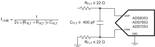 Figure 100. Antialiasing Filter
The input amplifier bandwidth should be much higher than the cutoff frequency of the antialiasing filter. TI strongly recommends performing a SPICE simulation to confirm that the amplifier has more than 40° phase margin with the selected filter. If an amplifier has less than a 40° phase margin with 22-Ω resistors, using a different amplifier with higher bandwidth or reducing the filter cutoff frequency with a larger differential capacitor is advisable.
9.2 Typical Applications
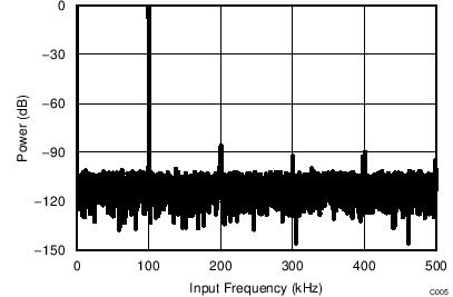
9.2.1 DAQ Circuit to Achieve Maximum SINAD for a 10-kHz Input Signal at Full Throughput
9.2.1.1 Design Requirements
To design an application circuit optimized to achieve target specifications listed in Table 20.
Table 20. Target Specifications
| TARGET SPECIFICATIONS | TEST CONDITIONS | ||||
|---|---|---|---|---|---|
| SNR | THD | DEVICE | INPUT SIGNAL FREQUENCY | THROUGHPUT | INTERFACE MODE |
| > 83 dB | < -100 dB | ADS8353 | 10 kHz | Maximum supported | 32-CLK, dual-SDO |
| > 81 dB | < –95 dB | ADS7853 | 10 kHz | Maximum supported | 32-CLK, dual-SDO |
| > 77.5 dB | < –85 dB | ADS7853 | 10 kHz | Maximum supported | 16-CLK, dual-SDO |
| > 71.5 dB | < –88 dB | ADS7253 | 10 kHz | Maximum supported | 32-CLK, dual-SDO |
| > 70.5 dB | < –80 dB | ADS7253 | 10 kHz | Maximum supported | 16-CLK, dual-SDO |
9.2.1.2 Detailed Design Procedure
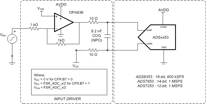
Best practice is for the distortion from the input driver to be at least 10 dB less than the ADC distortion. The distortion resulting from variation in the common-mode signal is eliminated by using the amplifier in an inverting gain configuration that establishes a fixed common-mode level for the circuit. This configuration also eliminates the requirement of rail-to-rail swing at the amplifier input. The low-power OPA836, used as an input driver, provides exceptional ac performance because of its extremely low-distortion and high-bandwidth specifications. In addition, the components of the antialiasing filter are such that the noise from the front-end circuit is kept low without adding distortion to the input signal.
The application circuit illustrated in Figure 101 is optimized to achieve the lowest distortion and lowest noise for a
10-kHz input signal fed to the ADS8353 or ADS7853 or ADS7253 operating at full throughput with the default 32-CLK, dual-SDO interface mode. The input signal is processed through a high-bandwidth, low-distortion amplifier in an inverting gain configuration and a low-pass RC filter before being fed into the device.
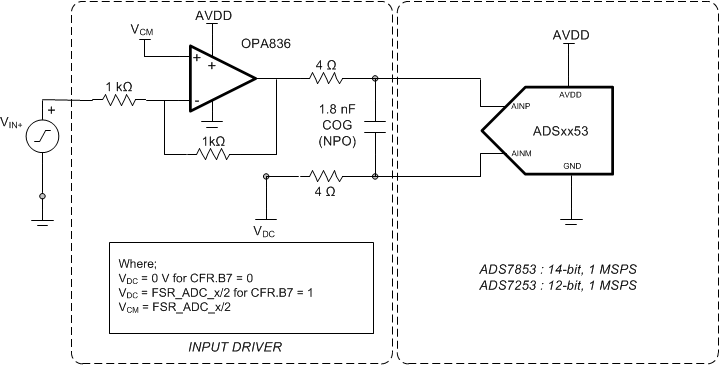
The ADS7853 and the ADS7253 also support 16-CLK interface modes that achieve the rated throughput rate at much lower SCLK frequencies. However, when using the 16-CLK interface modes, the device receives less acquisition time when compared to the 32-CLK interface modes. The application circuit illustrated in Figure 102 is optimized to achieve the lowest distortion and lowest noise for a 10-kHz input signal fed to the ADS7853 or ADS7253 operating at full throughput with the 16-CLK, dual-SDO interface mode. The input signal is processed through a high-bandwidth, low-distortion amplifier in an inverting gain configuration and a low-pass RC filter before being fed into the device.
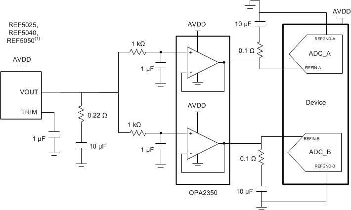
Figure 103 illustrates the reference driver circuit when operation with an external reference is desired. The reference voltage is generated by the high-precision, low-noise REF50xx circuit. The output broadband noise of the reference is heavily filtered by a low-pass filter with a 3-dB cutoff frequency of 160 Hz. The decoupling capacitor on each reference pin is selected to be 10 µF. The low output impedance, low noise, and fast settling time makes the OPA2350 a good choice for driving this high capacitive load.
9.2.1.3 Application Curves
To minimize external components and to maximize the dynamic range of the ADC, device is configured to operate with internal reference (CFR.B6 = 1) and 2 x VREF_x input full scale range (CFR.B9 = 1).
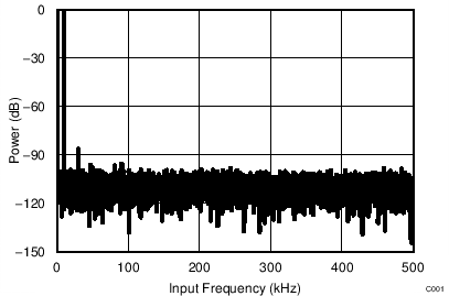
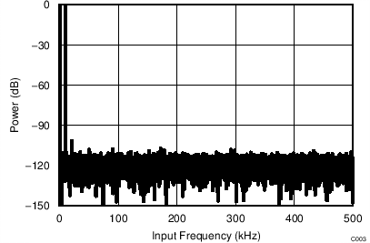
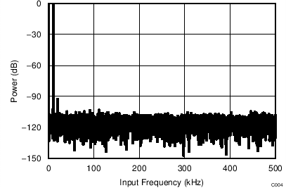
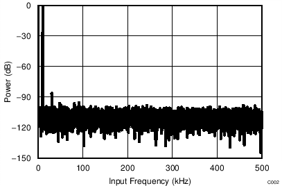
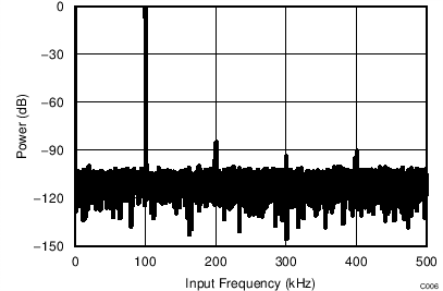
Figure 104, Figure 105, and Figure 106, show the FFT plots and test results obtained with the ADS8353, ADS7853, and ADS7253, respectively, operating at full throughput with a 32-CLK interface and the circuit configuration of Figure 101.
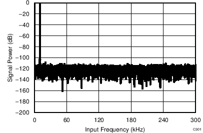
| SNR = 83.5 dB | THD = –101.2 dB | fIN = 10.1 kHz |
| SNR = 72.5 dB | THD = –94.2 dB | fIN = 10.1 kHz |
| SNR = 82.1 dB | THD = –98.2 dB | fIN = 10.1 kHz |
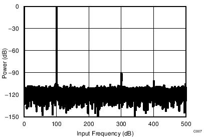
Figure 107 and Figure 108 show the FFT plots and test results obtained with the ADS7853 and ADS7253, respectively, operating at full throughput with 16-CLK interface and the circuit configuration of Figure 102.
| SNR = 78.1 dB | THD = –89.8 dB | fIN = 10.1 kHz |
| SNR = 71.2 dB | THD = –84.9 dB | fIN = 10.1 kHz |
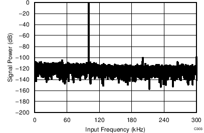
9.2.2 DAQ Circuit to Achieve Maximum SINAD for a 100-kHz Input Signal at Full Throughput
9.2.2.1 Design Requirements
To design an application circuit optimized to achieve target specifications listed in Table 21.
Table 21. Target Specifications
| TARGET SPECIFICATIONS | TEST CONDITIONS | ||||
|---|---|---|---|---|---|
| SNR | THD | DEVICE | INPUT SIGNAL FREQUENCY | THROUGHPUT | INTERFACE MODE |
| > 83 dB | < -95 dB | ADS8353 | 100 kHz | Maximum supported | 32-CLK, dual-SDO |
| > 78.5 dB | < –88 dB | ADS7853 | 100 kHz | Maximum supported | 32-CLK, dual-SDO |
| > 77.5 dB | < –85 dB | ADS7853 | 100 kHz | Maximum supported | 16-CLK, dual-SDO |
| > 71.5 dB | < –85 dB | ADS7253 | 100 kHz | Maximum supported | 32-CLK, dual-SDO |
| > 71 dB | < –84 dB | ADS7253 | 100 kHz | Maximum supported | 16-CLK, dual-SDO |
9.2.2.2 Detailed Design Procedure
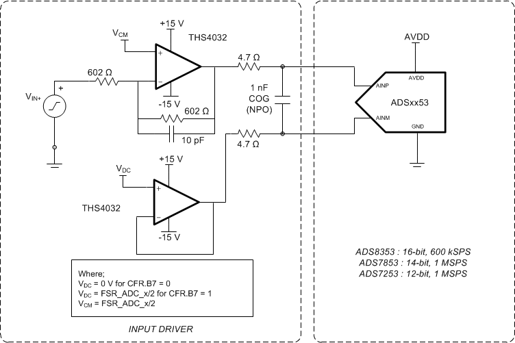
Best practice is for the distortion from the input driver to be at least 10 dB less than the ADC distortion. The distortion resulting from variation in the common-mode signal is eliminated by using the amplifier in an inverting gain configuration that establishes a fixed common-mode level for the circuit. This configuration also eliminates the requirement of rail-to-rail swing at the amplifier input. The low-power OPA836, used as an input driver, provides exceptional ac performance because of its extremely low-distortion and high-bandwidth specifications. In addition, the components of the antialiasing filter are such that the noise from the front-end circuit is kept low without adding distortion to the input signal. To take full advantage of the pseudo-differential input structure of the ADC, the AINM pin must be driven to the appropriate VDC with the same amplifier and matching source impedance.
The application circuit illustrated in Figure 109 is optimized to achieve the lowest distortion and lowest noise for a 100-kHz input signal fed to the ADS8353 or ADS7853 or ADS7253 operating at full throughput. The THS4032, used as an input driver, provides exceptional ac performance because of its extremely low-distortion, low-noise, and high-bandwidth specifications. In addition, the components of the antialiasing filter are such that the noise from the front-end circuit is kept low without adding distortion to the input signal. External clamp circuit may be required to ensure that the inputs to the device do not exceed AVDD.
Figure 103 illustrates the reference driver circuit when operation with an external reference is desired. The reference voltage is generated by the high-precision, low-noise REF50xx circuit. The output broadband noise of the reference is heavily filtered by a low-pass filter with a 3-dB cutoff frequency of 160 Hz. The decoupling capacitor on each reference pin is selected to be 10 µF. The low output impedance, low noise, and fast settling time makes the OPA2350 a good choice for driving this high capacitive load.
9.2.2.3 Application Curves
To minimize external components and to maximize the dynamic range of the ADC, device is configured to operate with internal reference (CFR.B6 = 1) and 2 x VREF_x input full scale range (CFR.B9 = 1).
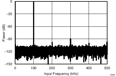
Figure 111, Figure 112, and Figure 113 show the FFT plots and test results obtained with the ADS8353, ADS7853 and ADS7253, respectively, operating at full throughput with a 32-CLK interface and the circuit configuration of Figure 109.
| SNR = 83.1 dB | THD = –95.5 dB | fIN = 100.2 kHz |
| SNR = 72.9 dB | THD = –85.8 dB | fIN = 100.2 kHz |
| SNR = 79.6 dB | THD = –90.9 dB | fIN = 100.2 kHz |
Figure 114 and Figure 115 show the FFT plots and test results obtained with the ADS7853 and ADS7253, respectively, operating with a 16-CLK interface and the circuit configuration of Figure 109.
| SNR = 78.2 dB | THD = –87.2 dB | fIN = 100.2 kHz |
| SNR = 72.3 dB | THD = –84.3 dB | fIN = 100.2 kHz |