SLOS729D October 2011 – November 2015 AFE5808A
PRODUCTION DATA.
- 1 Features
- 2 Applications
- 3 Description
- 4 Revision History
- 5 Description (continued)
- 6 Pin Configuration and Functions
- 7 Specifications
-
8 Detailed Description
- 8.1 Overview
- 8.2 Functional Block Diagram
- 8.3 Feature Description
- 8.4 Device Functional Modes
- 8.5 Programming
- 8.6
Register Maps
- 8.6.1 ADC Register Map
- 8.6.2
ADC Register/Digital Processing Description
- 8.6.2.1 AVERAGING_ENABLE: Address: 2[11]
- 8.6.2.2 ADC_OUTPUT_FORMAT: Address: 4[3]
- 8.6.2.3 DIGITAL_GAIN_ENABLE: Address: 3[12]
- 8.6.2.4 DIGITAL_HPF_ENABLE
- 8.6.2.5 DIGITAL_HPF_FILTER_K_CHX
- 8.6.2.6 LOW_FREQUENCY_NOISE_SUPPRESSION: Address: 1[11]
- 8.6.2.7 LVDS_OUTPUT_RATE_2X: Address: 1[14]
- 8.6.2.8 CHANNEL_OFFSET_SUBSTRACTION_ENABLE: Address: 3[8]
- 8.6.2.9 SERIALIZED_DATA_RATE: Address: 3[14:13]
- 8.6.2.10 TEST_PATTERN_MODES: Address: 2[15:13]
- 8.6.2.11 SYNC_PATTERN: Address: 10[8]
- 8.6.3 VCA Register Map
- 8.6.4 AFE5808A VCA Register Description
-
9 Application and Implementation
- 9.1 Application Information
- 9.2 Typical Application
- 9.3
Do's and Don'ts
- 9.3.1 Driving the Inputs (Analog or Digital) Beyond the Power-Supply Rails
- 9.3.2 Driving the Device Signal Input With an Excessively High Level Signal
- 9.3.3 Driving the VCNTL Signal With an Excessive Noise Source
- 9.3.4 Using a Clock Source With Excessive Jitter, an Excessively Long Input Clock Signal Trace, or Having Other Signals Coupled to the ADC or CW Clock Signal Trace
- 9.3.5 LVDS Routing Length Mismatch
- 9.3.6 Failure to Provide Adequate Heat Removal
- 10Power Supply Recommendations
- 11Layout
- 12Device and Documentation Support
- 13Mechanical, Packaging, and Orderable Information
Package Options
Mechanical Data (Package|Pins)
- ZCF|135
Thermal pad, mechanical data (Package|Pins)
Orderable Information
10 Power Supply Recommendations
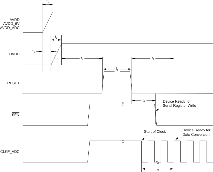
In a mixed-signal system design, power supply and grounding design plays a significant role. The AFE5808A device distinguishes between two different grounds: AVSS (analog ground) and DVSS (digital ground). In most cases, it should be adequate to lay out the printed-circuit-board (PCB) to use a single ground plane for the AFE5808A device. Take care to partition this ground plane properly between various sections within the system to minimize interactions between analog and digital circuitry. Alternatively, the digital (DVDD) supply set consisting of the DVDD and DVSS pins can be placed on separate power and ground planes. For this configuration, the AVSS and DVSS grounds should be tied together at the power connector in a star layout. In addition, optical isolator or digital isolators, such as ISO7240, can separate the analog portion from the digital portion completely. Consequently they prevent digital noise to contaminate the analog portion. Table 2 lists the related circuit blocks for each power supply. Recommended power up sequence is shown in Figure 93.

The AVDDx and DVDD power-on sequence does not matter as long as –10 ms < t3 < 10 ms. Similar considerations apply while shutting down the device.
Table 17. Supply vs Circuit Blocks
| POWER SUPPLY | GROUND | CIRCUIT BLOCKS |
|---|---|---|
| AVDD (3.3VA) | AVSS | LNA, attenuator, PGA with current clamp and BPF, reference circuits, CW summing amplifier, CW mixer, VCA SPI |
| AVDD_5V (5VA) | AVSS | LNA, CW clock circuits, reference circuits |
| AVDD_ADC (1.8VA) | AVSS | ADC analog and reference circuits |
| DVDD (1.8VD) | DVSS | LVDS and ADC SPI |
All bypassing and power supplies for the AFE5808A should be referenced to their corresponding ground planes. All supply pins should be bypassed with 0.1-µF ceramic chip capacitors (size 0603 or smaller). To minimize the lead and trace inductance, the capacitors should be located as close to the supply pins as possible. Where double-sided component mounting is allowed, these capacitors are best placed directly under the package. In addition, larger bipolar decoupling capacitors 2.2 µF to 10 µF, effective at lower frequencies) may also be used on the main supply pins. These components can be placed on the PCB in proximity (< 0.5 inch or 12.7 mm) to the AFE5808A device itself.
The AFE5808A device has a number of reference supplies needed to be bypassed, such as CM_BYP, and VHIGH. These pins should be bypassed with at least 1 µF; higher value capacitors can be used for better low-frequency noise suppression. For best results, choose low-inductance ceramic chip capacitors (size 0402, > 1 µF) and place them as close as possible to the device pins.
High-speed mixed signal devices are sensitive to various types of noise coupling. One primary source of noise is the switching noise from the serializer and the output buffer/drivers. For the AFE5808A device, the interaction between the analog and digital supplies within the device is ensured to keep to a minimal amount. The extent of noise coupled and transmitted from the digital and analog sections depends on the effective inductances of each of the supply and ground connections. Smaller effective inductance of the supply and ground pins leads to improved noise suppression. For this reason, multiple pins are used to connect each supply and ground sets. Take care to maintain low inductance properties throughout the design of the PCB layout by using proper planes and layer thickness.