SBAS585A September 2012 – January 2016 AMC1200-Q1
PRODUCTION DATA.
- 1 Features
- 2 Applications
- 3 Description
- 4 Revision History
- 5 Pin Configurations and Functions
- 6 Specifications
- 7 Detailed Description
- 8 Application and Implementation
- 9 Power Supply Recommendations
- 10Layout
- 11Device and Documentation Support
- 12Mechanical, Packaging, and Orderable Information
Package Options
Mechanical Data (Package|Pins)
Thermal pad, mechanical data (Package|Pins)
- DUB|8
Orderable Information
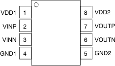
5 Pin Configurations and Functions
DUB and DWV Packages
8-Pin SOP and SOIC
Top View

Pin Functions
| PIN | I/O | DESCRIPTION | |
|---|---|---|---|
| NO. | NAME | ||
| 1 | VDD1 | — | High-side power supply, 4.5 V to 5.5 V. See the Power Supply Recommendations section for decoupling recommendations. |
| 2 | VINP | I | Noninverting analog input |
| 3 | VINN | I | Inverting analog input |
| 4 | GND1 | — | High-side analog ground |
| 5 | GND2 | — | Low-side analog ground |
| 6 | VOUTN | O | Inverting analog output with self-adjusting, common-mode voltage |
| 7 | VOUTP | O | Noninverting analog output with self-adjusting, common-mode voltage |
| 8 | VDD2 | — | Low-side power supply, 2.7 V to 5.5 V. See the Power Supply Recommendations section for decoupling recommendations. |