SBAS585A September 2012 – January 2016 AMC1200-Q1
PRODUCTION DATA.
- 1 Features
- 2 Applications
- 3 Description
- 4 Revision History
- 5 Pin Configurations and Functions
- 6 Specifications
- 7 Detailed Description
- 8 Application and Implementation
- 9 Power Supply Recommendations
- 10Layout
- 11Device and Documentation Support
- 12Mechanical, Packaging, and Orderable Information
Package Options
Mechanical Data (Package|Pins)
Thermal pad, mechanical data (Package|Pins)
- DUB|8
Orderable Information
9 Power Supply Recommendations
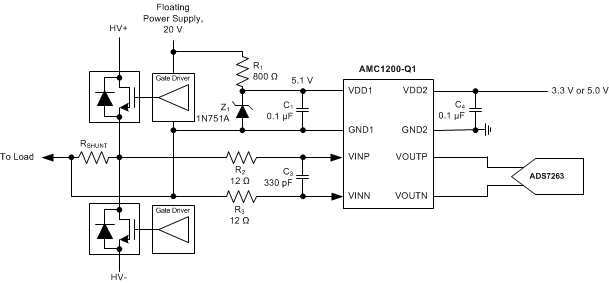
In a typical frequency inverter application, the high-side power supply for the AMC1200-Q1 (VDD1) is derived from the system supply, as shown in Figure 36. For lowest cost, a Zener diode can be used to limit the voltage to 5 V ± 10%. Using a 0.1-µF, low-ESR decoupling capacitor is recommended for filtering VDD1. Using a 0.1-µF decoupling capacitor is also recommended for filtering the power-supply on the VDD2 side. For best performance, place the decoupling capacitors (C1 and C4) as close as possible to the VDD1 and VDD2 pins, respectively. If better filtering is required, an additional 1-µF to 10-µF capacitor can be used in parallel to C1 and C4.
 Figure 36. Zener Diode Based High-Side Supply
For higher power efficiency and better performance, a buck converter can be used to generate VDD1; an example of such an approach is based on the LM5017. The PMP9480 reference design (Isolated Bias Supplies + Isolated Amplifier Combo for Line Voltage or Current Measurement) with performance test results and layout documentation is available from www.ti.com.
The AMC1200-Q1 does not require any particular power sequence and is operational when both power supplies, VDD1 and VDD2, are applied.