SLUSB97A October 2012 – December 2014
PRODUCTION DATA.
- 1 Features
- 2 Applications
- 3 Description
- 4 Revision History
- 5 Description (Continued)
- 6 Pin Configuration and Functions
- 7 Specifications
-
8 Detailed Description
- 8.1 Overview
- 8.2 Functional Block Diagram
- 8.3
Feature Description
- 8.3.1 Device Power Up
- 8.3.2 Power Path Management
- 8.3.3 Battery Charging Management
- 8.3.4 Status Outputs (STAT and INT)
- 8.3.5 Protections
- 8.3.6 Serial Interface
- 8.4 Device Functional Modes
- 8.5
Register Map
- 8.5.1
I2C Registers
- 8.5.1.1 Input Source Control Register REG00 (reset = 00110000, or 30)
- 8.5.1.2 Power-On Configuration Register REG01 (reset = 00011011, or 1B)
- 8.5.1.3 Charge Current Control Register REG02 (reset = 01100000, or 60)
- 8.5.1.4 Pre-Charge/Termination Current Control Register REG03 (reset = 00010001, or 11)
- 8.5.1.5 Charge Voltage Control Register REG04 (reset = 10110010, or B2)
- 8.5.1.6 Charge Termination/Timer Control Register REG05 (reset = 10011010, or 9A)
- 8.5.1.7 Thermal Regulation Control Register REG06 (reset = 00000011, or 03)
- 8.5.1.8 Misc Operation Control Register REG07 (reset = 01001011, or 4B)
- 8.5.1.9 System Status Register REG08
- 8.5.1.10 Fault Register REG09
- 8.5.1.11 Vender / Part / Revision Status Register REG0A (reset = 00100011, or 23)
- 8.5.1
I2C Registers
- 9 Application and Implementation
- 10Power Supply Recommendations
- 11Layout
- 12Device and Documentation Support
- 13Mechanical, Packaging, and Orderable Information
Package Options
Mechanical Data (Package|Pins)
- RGE|24
Thermal pad, mechanical data (Package|Pins)
- RGE|24
Orderable Information
6 Pin Configuration and Functions
RGE Package
24-Pin VQFN With Exposed Thermal Pad
(Top View)
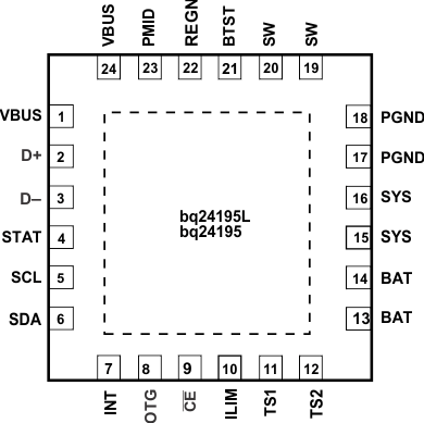
Pin Functions
| PIN | TYPE | DESCRIPTION | |
|---|---|---|---|
| NAME | NUMBER | ||
| VBUS | 1,24 | P | Charger Input Voltage. The internal n-channel reverse block MOSFET (RBFET) is connected between VBUS and PMID with VBUS on source. Place a 1-µF ceramic capacitor from VBUS to PGND and place it as close as possible to IC. (Refer to Application Information Section for details) |
| D+ | 2 | I Analog |
Positive line of the USB data line pair. D+/D– based USB host/charging port detection. The detection includes data contact detection (DCD) and primary detection in bc1.2. |
| D– | 3 | I Analog |
Negative line of the USB data line pair. D+/D– based USB host/charging port detection. The detection includes data contact detection (DCD) and primary detection in bc1.2. |
| STAT | 4 | O Digital |
Open drain charge status output to indicate various charger operation. Connect to the pull up rail via 10-kΩ. LOW indicates charge in progress. HIGH indicates charge complete or charge disabled. When any fault condition occurs, STAT pin blinks at 1 Hz. |
| SCL | 5 | I Digital |
I2C Interface clock. Connect SCL to the logic rail through a 10-kΩ resistor. |
| SDA | 6 | I/O Digital |
I2C Interface data. Connect SDA to the logic rail through a 10-kΩ resistor. |
| INT | 7 | O Digital |
Open-drain Interrupt Output. Connect the INT to a logic rail via 10-kΩ resistor. The INT pin sends active low, 256-us pulse to host to report charger device status and fault. |
| OTG | 8 | I Digital |
USB current limit selection pin during buck mode, and active high enable pin during boost mode. |
| In buck mode with USB host, when OTG = High, IIN limit = 500 mA and when OTG = Low, IIN limit = 100 mA. | |||
| The boost mode is activated when the REG01[5:4] = 10 and OTG pin is High. | |||
| CE | 9 | I Digital |
Active low Charge Enable pin. Battery charging is enabled when REG01[5:4] = 01 and CE pin = Low. CE pin must be pulled high or low. |
| ILIM | 10 | I Analog |
ILIM pin sets the maximum input current limit by regulating the ILIM voltage at 1 V. A resistor is connected from ILIM pin to ground to set the maximum limit as IINMAX = (1V/RILIM) × 530. The actual input current limit is the lower one set by ILIM and by I2C REG00[2:0]. The minimum input current programmed on ILIM pin is 500 mA. |
| TS1 | 11 | I Analog |
Temperature qualification voltage input #1. Connect a negative temperature coefficient thermistor. Program temperature window with a resistor divider from REGN to TS1 to GND. Charge suspends when either TS pin is out of range. Recommend 103AT-2 thermistor. TS1 and TS2 pins have to be shorted together. |
| TS2 | 12 | I Analog |
Temperature qualification voltage input #2. TS1 and TS2 pins have to be shorted together. |
| BAT | 13,14 | P | Battery connection point to the positive terminal of the battery pack. The internal BATFET is connected between BAT and SYS. Connect a 10 µF closely to the BAT pin. |
| SYS | 15,16 | P | System connection point. The internal BATFET is connected between BAT and SYS. When the battery falls below the minimum system voltage, switch-mode converter keeps SYS above the minimum system voltage. (Refer to Application Information Section for inductor and capacitor selection.) |
| PGND | 17,18 | P | Power ground connection for high-current power converter node. Internally, PGND is connected to the source of the n-channel LSFET. On PCB layout, connect directly to ground connection of input and output capacitors of the charger. A single point connection is recommended between power PGND and the analog GND near the IC PGND pin. |
| SW | 19,20 | O Analog |
Switching node connecting to output inductor. Internally SW is connected to the source of the n-channel HSFET and the drain of the n-channel LSFET. Connect the 0.047-µF bootstrap capacitor from SW to BTST. |
| BTST | 21 | P | PWM high side driver positive supply. Internally, the BTST is connected to the anode of the boost-strap diode. Connect the 0.047-µF bootstrap capacitor from SW to BTST. |
| REGN | 22 | P | PWM low side driver positive supply output. Internally, REGN is connected to the cathode of the boost-strap diode. Connect a 4.7-µF (10-V rating) ceramic capacitor from REGN to analog GND. The capacitor should be placed close to the IC. REGN also serves as bias rail of TS1 and TS2 pins. |
| PMID | 23 | P | Battery Boost Mode Output Voltage. Connected to the drain of the reverse blocking MOSFET and the drain of HSFET. The minimum capacitance required on PMID to PGND is 20 µF (bq24195L) or 60 µF (bq24195) |
| Thermal Pad | – | P | Exposed pad beneath the IC for heat dissipation. Always solder thermal pad to the board, and have vias on the thermal pad plane star-connecting to PGND and ground plane for high-current power converter. |