SLUSBY5G June 2014 – December 2015
UNLESS OTHERWISE NOTED, this document contains PRODUCTION DATA.
- 1 Features
- 2 Applications
- 3 Description
- 4 Revision History
- 5 Pin Configuration and Functions
- 6 Specifications
-
7 Detailed Description
- 7.1 Overview
- 7.2 Functional Block Diagram
- 7.3 Feature Description
- 7.4
Device Functional Modes
- 7.4.1 High Impedance Mode
- 7.4.2 Battery Only Connected
- 7.4.3 Input Connected
- 7.4.4 Battery Charging Process
- 7.4.5 Charge Time Optimizer
- 7.4.6 Battery Detection
- 7.4.7 Battery Overvoltage Protection (BOVP)
- 7.4.8 Dynamic Power Path Management
- 7.4.9 Battery Discharge FET (BGATE)
- 7.4.10 IUSB1, IUSB2, and IUSB3 Input
- 7.4.11 Safety Timer in Charge Mode
- 7.4.12 LDO Output (DRV)
- 7.4.13 External NTC Monitoring (TS)
- 7.4.14 Thermal Regulation and Protection
- 7.4.15 Status Outputs (CHG, PG)
- 7.4.16 Boost Mode Operation
- 8 Applications and Implementation
- 9 Power Supply Recommendations
- 10Layout
- 11Device and Documentation Support
- 12Mechanical, Packaging, and Orderable Information
Package Options
Mechanical Data (Package|Pins)
- RGE|24
Thermal pad, mechanical data (Package|Pins)
Orderable Information
1 Features
- Charge Time Optimizer (Enhanced CC/CV Transition) for Faster Charging
- Integrated FETs for Up to 3A Charge Rate at 5% Accuracy and 93% Peak Efficiency
- Boost Capability to Supply 5V at 1A at IN for USB OTG Supply
- Integrated Power Path MOSFET and optional BGATE control to Maximize Battery Life and Instantly Startup From a Deeply Discharged Battery or No Battery
- 30V Input Rating with Over-Voltage Protection Supports 5V USB2.0/3.0 and 12V USB Power Delivery
- Small Solution Size In a 4mm x 4mm QFN-24 Package
- Safe and Accurate Battery Management Functions Programmed Using IUSB and /CE
2 Applications
- Handheld Scanner and Point of Sale Terminals
- Handheld Products
- Power Banks and External Battery Packs
- Small Power Tools
- Portable Media Players and Gaming
3 Description
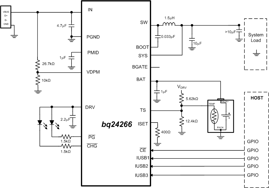
The bq24266 is highly integrated single cell Li-Ion battery charger and system power path management devices that supports operation from either a USB port or wall adapter supply. The power path feature allows the bq24266 to power the system from a high efficiency DC to DC converter while simultaneously and independently charging the battery. The power path also permits the battery to supplement the system current requirements when the adapter cannot. To support USB OTG applications, the bq24266 is configurable to boost the battery voltage to 5V and supply up to 1A at the input. The battery is charged with three phases: precharge, constant current and constant voltage. Thermal regulation prevents the die temperature from exceeding 125°C. Additionally, a JEITA compatible battery pack thermistor monitoring input (TS) is included to prevent the battery from charging outside of its safe temperature range.
Device Information(1)
| PART NUMBER | PACKAGE | BODY SIZE (NOM) |
|---|---|---|
| bq24266 | VQFN (24) | 4.00mm × 4.00mm |
- For all available packages, see the orderable addendum at the end of the datasheet.
